Tiếng Việt
 日本語
日本語The global GaN fast charger market is projected to reach $3.2B by 2027 — growing at 28% CAGR. Behind every 65W GaN charger that fits in a shirt pocket is a power PCB assembly that had to solve switching frequencies above 1MHz, creepage distances at 265VAC input, and USB-C PD 3.1 compliance — all on a board smaller than a credit card. If you are a Hardware Engineer or Product Manager developing or outsourcing a GaN fast charger program, this guide covers everything your assembly partner needs to get right: DFM rules, thermal management, certification requirements, and how to qualify a power PCB assembly supplier that actually understands the discipline. For SHDC’s production experience with GaN fast chargers, see our GaN charger manufacturing capabilities.
Why Fast Charger Power PCB Assembly Is a Different Discipline

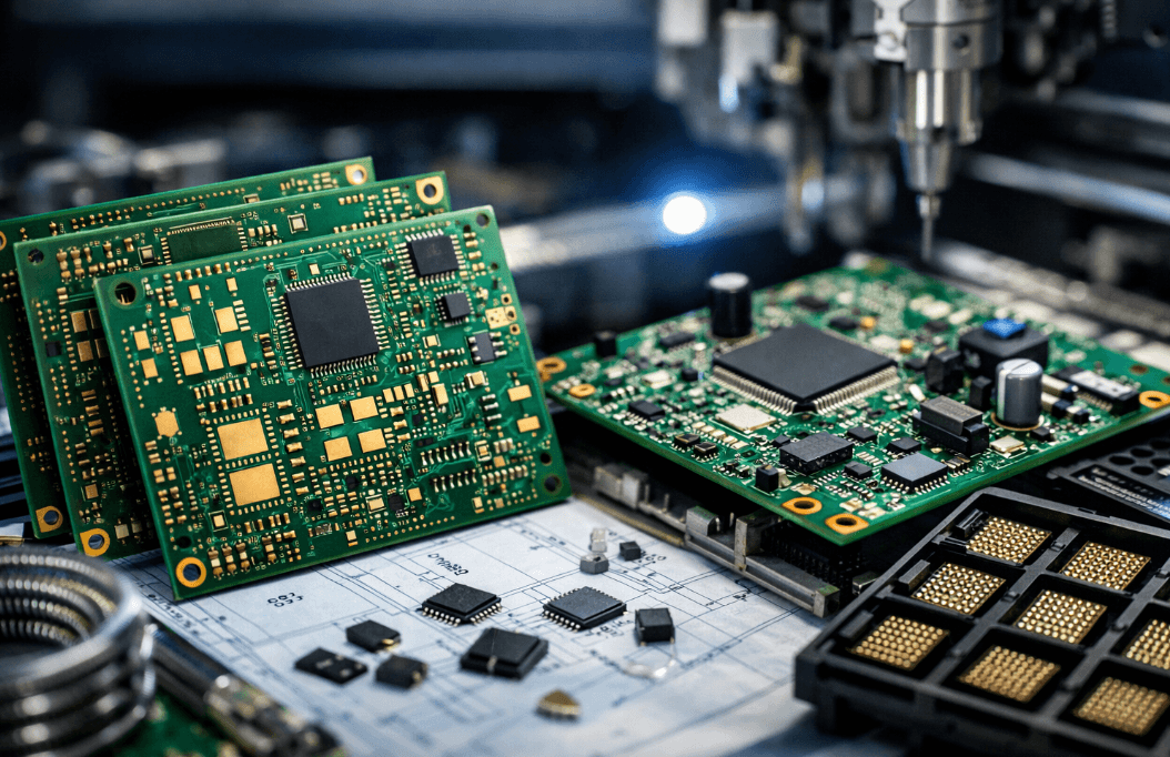
Standard consumer electronics PCBA and power PCB assembly for fast chargers share the same SMT equipment — but almost nothing else. The physics of high-voltage AC input, GaN switching at megahertz frequencies, and USB-C Power Delivery negotiation create a set of design and process constraints that most standard EMS providers are not equipped to handle. Understanding what makes this discipline unique is the first step in qualifying the right assembly partner.
The GaN Revolution Changed Everything on the PCB
Silicon MOSFETs dominated charger design for decades — switching at 65–200kHz, requiring large transformers and bulky filter capacitors. GaN FETs changed the equation fundamentally. Operating at switching frequencies above 1MHz, GaN enables transformers and passives to shrink by 60–70% — which is why a 65W GaN charger fits in a form factor that a 65W silicon charger never could.
But that miniaturization creates direct PCB layout challenges:
- Gate drive loop area must be minimized to below 0.5cm² — any parasitic inductance in the gate loop causes ringing, false turn-on, and EMI failures
- Power switching loop — GaN FET, bootstrap capacitor, output capacitor — must be kept below 1cm² loop area
- Component density increases dramatically — fine-pitch QFN and DFN packages replace larger through-hole devices
- EMI becomes a first-order design constraint, not an afterthought — GaN switching harmonics at 1MHz+ require careful layout to pass FCC Part 15 and CE EMC testing
According to Yole Group’s GaN Power Device Market Monitor (2024), GaN-based charger shipments exceeded 800M units in 2024 — with the majority manufactured in Asia. The power PCB assembly discipline supporting this volume is concentrated in a small number of manufacturers who have invested in the process knowledge to execute it reliably.
USB-C PD 3.1 Adds Complexity Beyond Power
USB-C Power Delivery 3.1 extends output voltage to 48V and power to 240W — but even a standard 65W USB-C PD charger carries significant board-level complexity beyond the power stage:
- Multiple output profiles: 5V/3A, 9V/3A, 15V/3A, 20V/5A — the PD controller IC negotiates dynamically, requiring the power stage to regulate across a wide voltage range
- CC pin logic: USB-C CC pins carry PD communication — ESD protection placement within 0.5mm of the port is mandatory to avoid trace inductance degrading protection effectiveness
- E-Marker cable detection: 100W+ programs require E-Marker cable detection logic on the board
- Safety ICs: UL 62368-1 and CE certification require dedicated overvoltage, overcurrent, and over-temperature protection ICs — placement and routing of these ICs directly affects certification outcome
For a deeper look at consumer electronics PCB assembly requirements, see SHDC’s consumer electronics PCB assembly capabilities.
Safety Standards That Govern the PCB Design
The PCB layout of a fast charger is not a free design choice — it is directly constrained by the safety standards required for market access:
| Standard | Market | Key PCB Requirement |
|---|---|---|
| UL 62368-1 | USA / Canada | Creepage, clearance, flammability rating |
| CE (LVD + EMC) | European Union | Isolation, EMC layout rules |
| FCC Part 15 | USA | EMI — GaN switching harmonics |
| USB-IF TID | Global | USB PD compliance at board level |
| PSE | Japan | Stricter creepage than UL |
| KC | Korea | Similar to UL 62368-1 |
IEC 62368-1, which replaced both IEC 60950-1 and IEC 60065, is now the governing standard for fast charger safety globally. Every creepage distance, clearance gap, and isolation barrier on the PCB must be designed to this standard — or the product will not pass certification regardless of how well the power stage performs.
DFM Rules for Fast Charger Power PCB Assembly
This is where most power PCB assembly programs succeed or fail. DFM errors in fast charger PCBs are not caught by standard AOI — they show up in certification testing, thermal failures in the field, or EMI failures at the pre-compliance lab. A supplier who returns a DFM report with no issues found in under four hours has not reviewed your files.
Creepage & Clearance at 265VAC Input
For a consumer fast charger operating at 265VAC input (universal input range), the isolation requirements between primary and secondary sides are non-negotiable:
- Pollution degree 2, Overvoltage Category II — standard classification for consumer charger
- Basic insulation: minimum 3.2mm creepage at 265VAC
- Reinforced insulation (required primary-to-secondary): minimum 6.4mm creepage — this is the number that drives PCB layout decisions
- When PCB real estate cannot provide 6.4mm of surface creepage, slot routing through the PCB substrate is required — this must be specified explicitly in fabrication notes, not assumed
The primary-to-secondary boundary on the PCB must be treated as a hard design constraint from the first schematic capture, not a layout afterthought. According to IPC-2221B Table 6-1, these values are minimum requirements — your certification lab may require additional margin.
High-Frequency Layout Rules for GaN Switching Stage
GaN layout is the highest-risk area in fast charger power PCB assembly — and the area where the gap between a capable and an incapable supplier is most visible:
- Power loop: GaN FET drain → output capacitor → GaN FET source — loop area must be below 1cm². Every mm² of additional loop area adds parasitic inductance, increases voltage overshoot, and worsens EMI
- Gate drive loop: Gate driver output → GaN FET gate → GaN FET Kelvin source → gate driver return — separate layer, below 0.5cm² loop area
- Kelvin source connection: GaN FETs with exposed Kelvin source pin require a dedicated PCB connection separate from the power source — this eliminates power loop current from the gate drive return path, reducing switching noise by 30–50%
- Ground plane splitting: Primary GND and secondary GND must connect at a single point — typically at the transformer secondary return. Multiple connection points create ground loops that fail EMC testing
A useful reference for GaN layout best practices is Texas Instruments’ GaN layout application note SLPA010 — the principles apply regardless of GaN FET vendor.
Thermal Management on a Miniaturized Power PCB
A 65W GaN charger dissipates approximately 3–4W as heat — in a volume smaller than 50cm³. The thermal path from GaN FET junction to ambient must be engineered at the PCB level:
- Thermal via array: Minimum 9 vias under the GaN FET thermal pad, 0.3mm diameter, copper-filled preferred. Unfilled vias reduce thermal conductivity by 40–60% compared to copper-filled
- Copper pour: Solid pour on the layer directly below the GaN FET — hatched pour reduces thermal conductivity and should not be used in the thermal dissipation path
- Operating temperature derating: Inside a charger enclosure at full load, ambient temperature reaches 75–85°C. All component ratings must be verified at this temperature — not at 25°C datasheet conditions
- Transformer thermal: The transformer is typically the highest-temperature component — placement must allow airflow or conduction path to the enclosure
Thermal void formation in the GaN FET solder joint is the most common assembly-related thermal failure. IPC-7093 defines the acceptance criterion: void area must not exceed 25% of the thermal pad area. This requires X-ray inspection — not AOI.
Component Placement Rules
Placement sequence for fast charger power PCB assembly follows thermal and electrical priority, not mechanical convenience:
- Transformer: Center of board preferred — minimizes primary and secondary trace lengths simultaneously
- Input filter capacitors: Within 5mm of AC input — minimize the EMI current loop at the input
- GaN FET: Adjacent to transformer primary winding termination — minimize switching loop
- Output capacitors: Within 3mm of output connector — minimize output ripple
- Opto-coupler: Straddles primary/secondary boundary — placement must maintain ≥8mm creepage between primary and secondary pins while keeping feedback loop short
- ESD protection (USB-C): Within 0.5mm of USB-C port pins — trace inductance between TVS and port degrades ESD protection effectiveness
DFM Checklist — Fast Charger Power PCB Assembly
Use this checklist before submitting files to any power PCB assembly supplier. A qualified supplier should independently identify all items flagged below:
| # | DFM Check | Pass Criteria | Common Failure Mode |
|---|---|---|---|
| 1 | Creepage primary→secondary | ≥6.4mm reinforced insulation | <3.2mm, no slot specified |
| 2 | GaN power loop area | <1cm² | >3cm², EMI/overshoot |
| 3 | Gate drive loop area | <0.5cm² | Shared with power loop |
| 4 | Thermal via array (GaN) | ≥9 vias/cm², copper-filled | Too sparse, unfilled |
| 5 | Ground plane split | Single-point connection | Multiple connections, EMC fail |
| 6 | ESD protection (USB-C) | TVS within 0.5mm of port | Far from port, trace inductance |
| 7 | Opto-coupler clearance | ≥8mm primary→secondary | Insufficient isolation |
| 8 | Input cap placement | Within 5mm of AC input | Far, large EMI loop |
| 9 | Test point access | ≥2.54mm grid, ICT-accessible | Blocked by components |
| 10 | Conformal coat keepout | Defined on fabrication drawing | Missing, coating connectors |
| 11 | Slot routing specification | Explicit in fab notes if <6.4mm | Assumed, not specified |
| 12 | Transformer clearance | ≥2mm from board edge | Mechanical interference |
| 13 | GaN FET orientation | Thermal pad toward heatsink path | Random orientation |
| 14 | Kelvin source connection | Dedicated trace, not shared | Shared with power source |
| 15 | Output voltage sense | Kelvin connection at output cap | Sensed at connector, inaccurate |
PCB Stack-Up & Materials for Fast Charger Power PCB Assembly
The fabrication specification is as important as the assembly process for fast charger power PCB assembly. A board built to the wrong material specification will fail thermally or electrically regardless of assembly quality.
Layer Count & Stack-Up Recommendation
- 2-layer boards: Acceptable only for chargers below 30W with silicon topology — not recommended for GaN
- 4-layer minimum for GaN chargers ≥45W: The additional layers are not a cost luxury — they are required to implement separate power and gate drive loops without interference
- Recommended 4-layer stack-up:
- Layer 1: Signal + Power components (SMT side)
- Layer 2: Ground plane (primary GND + secondary GND, split)
- Layer 3: Power plane (secondary output distribution)
- Layer 4: Signal + THT component side
- Impedance control: Not required for power stage — but required for USB-C CC pins: 90Ω differential impedance per USB-C specification Rev 2.1
PCB Material Selection
| Material | Application | Tg | Cost Index |
|---|---|---|---|
| FR4 standard | Chargers ≤45W, good thermal design | 130–140°C | 1.0x |
| High-Tg FR4 | Chargers >65W, recommended | ≥170°C | 1.3x |
| Halogen-free FR4 | EU RoHS mandatory | ≥150°C | 1.4x |
| Rogers 4350B | RF/microwave — not needed for charger | N/A | 8x+ |
For most fast charger programs, High-Tg halogen-free FR4 is the correct specification — it satisfies EU RoHS, handles the thermal environment, and does not carry the cost premium of specialty materials.
Copper weight recommendation: 1oz standard for signal and control layers, 2oz for primary power traces carrying >3A — specify explicitly in the fabrication drawing, not assumed.
Surface Finish Impact on Assembly
| Surface Finish | Pros | Cons | Recommendation |
|---|---|---|---|
| ENIG | Flat, excellent for fine-pitch QFN/DFN | Cost premium | ✅ Preferred for GaN packages |
| HASL (lead-free) | Low cost, robust | Not flat — fine-pitch risk | ⚠️ Acceptable for THT-heavy boards |
| OSP | Low cost, flat | 6-month shelf life | ⚠️ Only if assembly within 3 months |
| ENEPIG | Best for Au wire bond | Significant cost premium | ❌ Overkill for charger |
ENIG is the correct specification for fast charger power PCB assembly — GaN QFN and DFN packages require a flat, solderable surface for consistent thermal pad contact.
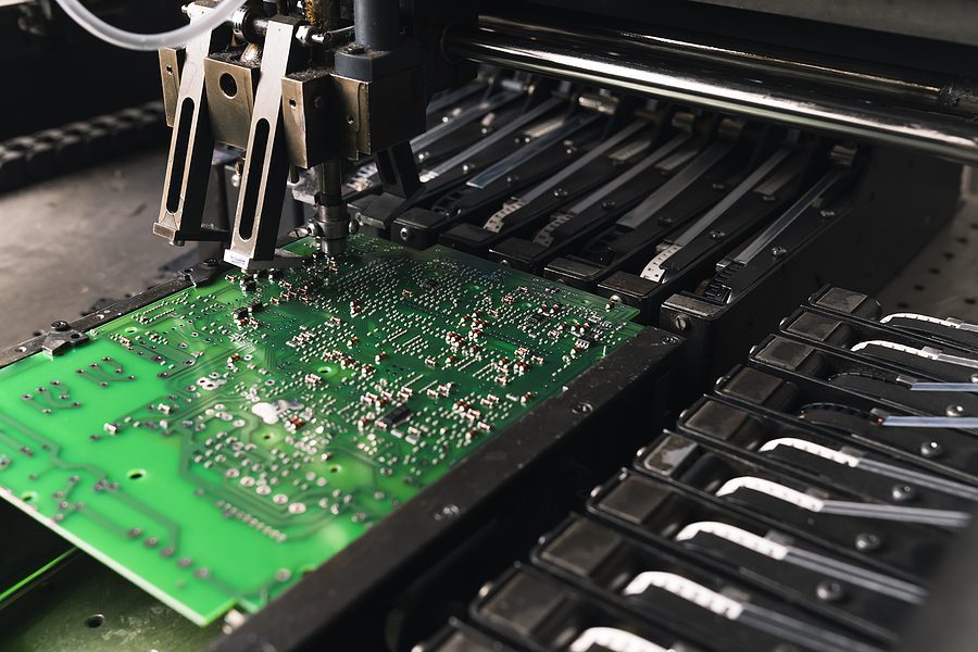
Assembly Process — What Happens on the Production Line
Understanding the production process helps Hardware Engineers write better assembly specifications and identify capability gaps during supplier qualification.
Solder Paste & Stencil for GaN Components
Stencil design for GaN packages is one of the most common sources of assembly defects in fast charger power PCB assembly:
- QFN/DFN aperture reduction: Reduce stencil aperture to 80–85% of pad size — full aperture causes solder bridging under the package
- Thermal pad aperture: Use array pattern (9–16 openings) rather than single aperture — controls paste volume and prevents voiding
- Stencil thickness: 0.12mm for fine-pitch GaN packages — 0.15mm standard stencil deposits too much paste
- SAC305 alloy: Standard for RoHS-compliant fast charger assembly — adequate reliability for consumer thermal cycling profile
For SHDC’s SMT process capabilities including stencil design support, see SMT assembly services at SHDC.
Reflow Profile for Power Components
The reflow profile for fast charger boards must balance competing thermal requirements:
- GaN FET: Follow JEDEC J-STD-020 moisture sensitivity level — preheat ramp rate ≤3°C/second
- Transformer: Large thermal mass requires extended soak zone (150–180°C for 60–90 seconds) to ensure uniform temperature before reflow
- Peak temperature: 245–250°C for SAC305 — verify all components are rated for this peak
- Nitrogen atmosphere: Strongly recommended for GaN QFN packages — improves wetting on thermal pad, reduces void formation by 15–25%
- Assembly sequence: SMT reflow first (GaN FET, controller ICs, passives), then selective soldering for THT components (AC input connector, electrolytic capacitors, fuse holder)
Selective Soldering for THT Components
Fast charger boards typically contain 4–8 through-hole components that cannot be wave soldered without thermal damage to adjacent SMT components:
- Selective solder vs wave solder: Selective soldering is mandatory — wave soldering exposes the entire board to solder contact, damaging fine-pitch SMT components
- Flux selection: No-clean flux per IPC J-STD-004 — eliminates cleaning step, compatible with conformal coating adhesion
- Preheat: 100–120°C board temperature before selective solder contact — prevents thermal shock to PCB substrate
Inspection & Testing Protocol
A complete inspection and test protocol for fast charger power PCB assembly includes six stages — each catching failure modes the previous stage cannot:
- 3D SPI (Solder Paste Inspection): 100% inspection post-stencil print — catches insufficient paste on GaN thermal pad before reflow. Critical: thermal pad paste volume directly determines void percentage
- 3D AOI post-reflow: 100% inspection — detects tombstoning, solder bridging, missing components, polarity errors
- X-ray inspection: GaN QFN and BGA void inspection per IPC-7093 — void area must not exceed 25% of thermal pad. 2D X-ray is minimum; 3D CT X-ray preferred for high-volume programs
- ICT (In-Circuit Test): Full electrical net coverage — verifies component values, orientation, and isolation resistance between primary and secondary (minimum 100MΩ)
- Hi-pot test: 3000VAC for 1 second between primary and secondary — mandatory per IEC 62368-1 before functional test. Any breakdown indicates creepage violation or contamination
- Functional load test: 100% rated power for minimum 5 minutes — measure output voltage accuracy (±1%), efficiency (target >92% for GaN), and temperature rise at GaN FET
For SHDC’s quality control process details, see PCB assembly quality control at SHDC.
Certifications Required for Fast Charger Power PCB Assembly
Certification is not a post-production activity — it is a design constraint that must be embedded in the PCB layout from day one. Hardware teams that treat certification as a final step routinely discover layout violations that require board respins, adding 8–16 weeks to their program timeline.
Product-Level Certifications
| Certification | Market | Governing Body | Key PCB-Level Requirement |
|---|---|---|---|
| UL 62368-1 | USA / Canada | UL Solutions | Creepage, clearance, flammability (UL94 V-0) |
| CE (LVD + EMC) | European Union | Notified Body | Isolation barriers, EMC layout |
| FCC Part 15 | USA | FCC | Conducted + radiated emissions — GaN harmonics |
| USB-IF TID | Global | USB-IF | USB PD protocol compliance |
| PSE (J-mark) | Japan | METI | Creepage requirements stricter than UL |
| KC | South Korea | KATS | Equivalent to UL 62368-1 |
| BIS | India | BIS | Growing requirement for India market entry |
Critical insight for Hardware Engineers: PSE (Japan) requires stricter creepage distances than UL 62368-1. If your program targets Japan, design to PSE creepage requirements from the start — do not design to UL and attempt to retrofit for PSE. The layout changes required are typically not minor.
IPC Standards Applicable to Fast Charger PCB Assembly
- IPC-A-610 Class 2: Minimum acceptable standard for consumer fast charger — defines solder joint acceptability criteria
- IPC-A-610 Class 3: Recommended for premium or enterprise-grade chargers — zero tolerance for safety-critical solder joint defects, 100% inspection at every stage
- IPC-J-STD-001: Soldering process requirements — flux classification, process control, operator qualification
- IPC-7711/7721: Rework and repair standard — important during NPI iteration cycles when board respins are frequent
- IPC-2221B: PCB design standard — creepage and clearance tables used directly in certification
How SHDC Supports Certification

- Pre-compliance EMC scan: SHDC conducts pre-compliance EMC screening before samples are submitted to certification labs — typically catches 1–2 layout issues that would otherwise cause lab failures, saving 6–10 weeks of iteration time
- Hi-pot test in-house: 100% hi-pot testing at 3000VAC verifies primary-to-secondary isolation before samples leave the factory — certification labs receive boards that have already passed the most common failure mode
- Documentation package: Full traceability documentation, component origin records, and test reports provided with each sample batch
For SHDC’s full quality and certification capabilities, see SHDC quality and certifications.
Sourcing Fast Charger Power PCB Assembly in Vietnam — The Cost Case
Vietnam’s cost advantage for fast charger power PCB assembly is more significant than for standard consumer electronics PCBA — for a structural reason that is often overlooked.
The Tariff Math for Fast Chargers
Fast chargers classify under HTS 8504.40 (static converters) — currently subject to 145% Section 301 tariff from China, versus 0% MFN rate from Vietnam:
| Cost Component | China-sourced | Vietnam-sourced |
|---|---|---|
| Factory unit cost (65W GaN) | $8.00 | $8.40 |
| Tariff (145% vs 0%) | $11.60 | $0.00 |
| Freight + logistics | $0.80 | $0.90 |
| Total landed cost | $20.40 | $9.30 |
| Tariff savings per unit | — | $11.10 |
At 50,000 units per month, the tariff differential alone is $555,000/month — $6.66M annually on a single SKU. The Vietnam factory unit cost premium of $0.40 is economically irrelevant against this differential.
For a comprehensive tariff analysis across electronics categories, see China vs Vietnam tariff impact for US OEMs.
Why Fast Chargers Benefit More Than Standard PCBA
Fast charger power PCB assembly is more labor-intensive than pure SMT programs — and Vietnam’s labor cost advantage compounds accordingly:
- THT components (AC input connector, electrolytic capacitors, fuse holder): selective soldering and manual inspection are labor-intensive operations where Vietnam’s $2.50–$4.00/hour fully-loaded labor rate creates a larger absolute saving than on pure SMT programs
- Functional test and hi-pot test: Both require operator involvement — manual test station operation at Vietnam labor rates versus China rates represents meaningful per-unit cost difference at volume
- NPI iteration cycles: Vietnam-based suppliers with engineering capability can support DFM iteration at lower cost per cycle — important for programs with 3–5 board respins before production release
SHDC’s Specific Advantage — Production Experience, Not Capability Claims
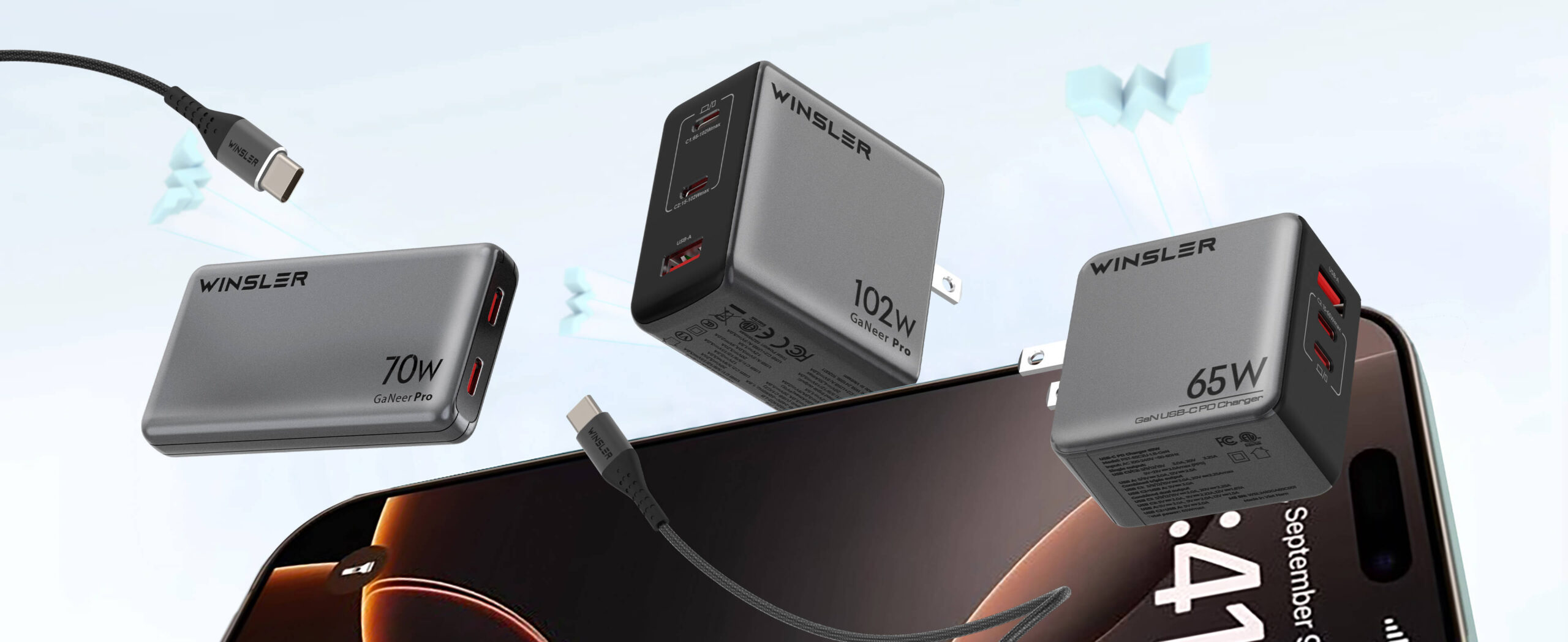
SHDC manufactures the Winsler GaN fast charger series — 65W to 150W GaN chargers under its own brand. This is not a capability claim — it is documented production history with the exact product type this guide covers. The process knowledge, DFM database, and test protocols described in this guide are drawn from active production programs, not theoretical capability.
SHDC operates from VSIP Hai Duong Industrial Zone — 55km from Hai Phong deep-water port, with 18–22 day transit time to US West Coast ports. Zero UFLPA geographic exposure. Full component origin documentation available on demand.
FAQs
What makes GaN fast charger PCB assembly different from standard PCBA?
GaN fast charger power PCB assembly operates at switching frequencies above 1MHz — versus 65–200kHz for silicon designs. This requires minimized power and gate drive loop areas (<1cm² and <0.5cm² respectively), thermal via arrays under GaN packages, and primary-to-secondary creepage of ≥6.4mm for reinforced insulation at 265VAC. Standard EMS suppliers without specific GaN experience routinely miss these requirements in DFM review.
What IPC standard applies to consumer fast charger PCB assembly?
IPC-A-610 Class 2 is the minimum standard for consumer fast charger power PCB assembly. Class 3 is recommended for premium or enterprise-grade chargers. IPC-J-STD-001 governs the soldering process. IPC-2221B provides the creepage and clearance tables referenced in UL 62368-1 certification.
How do I specify creepage distance for a 65W USB-C charger PCB?
For a 65W USB-C charger with 265VAC universal input, specify reinforced insulation between primary and secondary: minimum 6.4mm creepage per IPC-2221B Table 6-1 at Pollution Degree 2, Overvoltage Category II. If PCB real estate cannot provide 6.4mm surface creepage, specify slot routing in fabrication notes — do not assume the PCB fabricator will add slots without explicit instruction.
Can Vietnam manufacturers handle GaN fast charger power PCB assembly?
Yes — qualified Vietnam EMS providers with GaN production experience handle this discipline routinely. The key differentiator is not geography but process capability: nitrogen reflow, copper-filled thermal vias, 3D X-ray for void inspection, and hi-pot testing. SHDC’s Winsler GaN charger production (65W–150W) is direct evidence of this capability in Vietnam. See GaN charger manufacturing at SHDC for production details.
What is the typical MOQ and lead time for fast charger power PCB assembly in Vietnam?
Standard production lead time for fast charger power PCB assembly at SHDC is 3–5 weeks from approved BOM and Gerber files. Quick-turn prototype builds run 1–2 weeks. MOQ for production programs is typically 500–1,000 units depending on component availability. NPI programs can start from 50–100 units for first article builds.
Conclusion
Fast charger power PCB assembly is a discipline that rewards suppliers who understand the physics — GaN switching behavior, creepage requirements, thermal via design, and USB-C PD compliance are not details that can be learned on your program’s first build. SHDC brings documented GaN charger production experience, in-house hi-pot testing, X-ray void inspection, and Vietnam’s structural cost advantage to every fast charger program. The combination of technical depth and tariff-optimized location is not common — and it is what separates a qualification-ready supplier from an aspirational one.