Tiếng Việt
 日本語
日本語In modern electronics, almost every device—from smartphones and medical equipment to automotive systems and industrial controllers—relies on PCBA. Despite being a common term in manufacturing, many people still confuse PCBA with PCB, leading to misunderstandings when sourcing or designing electronic products.
In this guide, you’ll learn what PCBA is, how the PCBA assembly process works, the difference between PCB vs. PCBA, common PCBA testing methods, applications, and cost factors. This article is designed for beginners, engineers, and businesses looking for reliable PCBA manufacturing services.
What is PCBA?
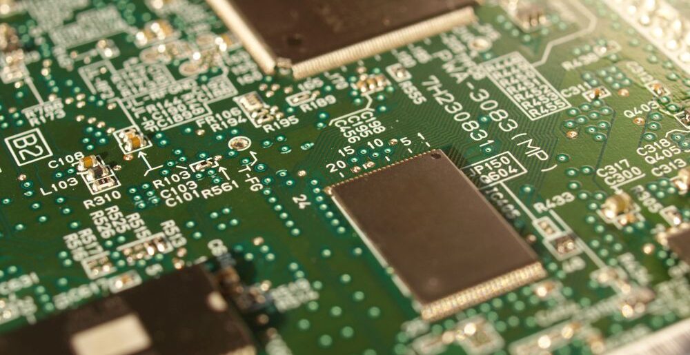
PCBA stands for Printed Circuit Board Assembly. PCBA refers to a fully assembled printed circuit board that has undergone the complete electronics manufacturing process, including:
-
Fabrication of the PCB (Printed Circuit Board)
-
Assembly of electronic components using SMT and/or THT (DIP) technologies
-
Precision soldering, optical inspection, and comprehensive functional testing
As the final output in the PCB manufacturing lifecycle, PCBA is ready for direct integration into electronic products such as control systems, power supplies, IoT devices, industrial machinery, and medical equipment.
By adhering to strict quality control standards, IPC guidelines, and functional testing procedures, professional PCBA/SMT manufacturers ensure reliable performance, long-term durability, and consistent product quality across prototypes, low-volume, and mass production.
PCB vs. PCBA: What’s the difference?
Many customers—especially hardware startups or companies outsourcing electronics manufacturing for the first time—often confuse PCB with PCBA. This misunderstanding can result in incomplete quotation requests or an incorrect interpretation of the manufacturer’s scope of work.
What is a PCB?
A PCB (Printed Circuit Board) is a bare circuit board that consists only of:
-
The base substrate material (such as FR4, aluminum, CEM, etc.)
-
Conductive copper layers
-
Drilled holes, component pads, solder mask, and silkscreen
A PCB does not have any electronic components assembled on it and therefore cannot function on its own. It serves solely as the mechanical and electrical foundation for electronic components such as ICs, resistors, capacitors, and diodes.
Detailed comparison: PCB vs PCBA
| Criteria | PCB | PCBA |
|---|---|---|
| Components | No components assembled | Fully assembled with electronic components |
| Functionality | Not functional | Fully functional according to design |
| Manufacturing Stage | Initial stage | Final stage |
| Process | PCB fabrication only | SMT, THT (DIP), soldering, inspection, and functional testing |
| Cost | Lower | Higher (includes components, assembly, and testing) |
| Application | Serves as a base for assembly | Ready for integration into end products |
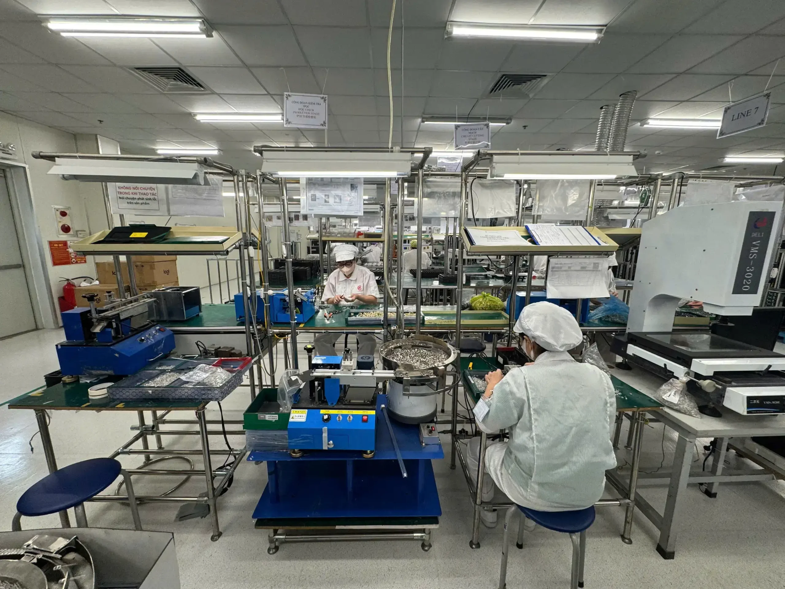
PCBA assembly process: Step-by-step manufacturing workflow
The PCBA assembly process consists of multiple critical stages designed to ensure product quality, electrical reliability, and long-term performance. A well-controlled PCBA process not only minimizes defects but also guarantees that the assembled circuit boards meet design specifications and industry standards such as IPC.
Below is a detailed breakdown of the standard PCBA manufacturing workflow used by professional SMT and electronics manufacturing service (EMS) providers.
1. Manufacturing Data Preparation
Before any physical assembly begins, accurate and complete production data is essential. This stage directly impacts assembly accuracy, yield rate, and production lead time.
Required manufacturing files typically include:
-
Gerber files – Define PCB layout, copper layers, solder mask, and silkscreen
-
BOM (Bill of Materials) – Lists all electronic components, part numbers, specifications, and quantities
-
Pick-and-place files – Specify exact component placement coordinates and rotation angles for SMT machines
Accurate and validated data helps manufacturers:
-
Prevent component placement errors
-
Avoid material mismatches
-
Reduce production delays and rework costs
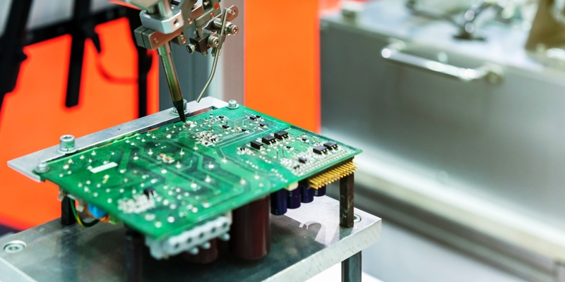
2. SMT Assembly (Surface Mount Technology)
SMT assembly is the most widely used method in modern electronics manufacturing due to its efficiency, precision, and scalability.
The SMT process typically includes:
a. Solder Paste Printing
A stainless steel stencil is used to apply solder paste accurately onto PCB pads. Proper paste volume and alignment are critical for reliable solder joints.
b. Automated SMD Component Placement
High-speed pick-and-place machines mount surface-mount devices (SMDs) onto the PCB with high positional accuracy.
c. Reflow Soldering
The assembled board passes through a reflow oven, where controlled temperature profiles melt the solder paste, forming strong and consistent electrical connections.
Advantages of SMT assembly include:
-
High component density
-
Compact PCB design
-
Lower manufacturing cost at scale
-
High repeatability and production efficiency
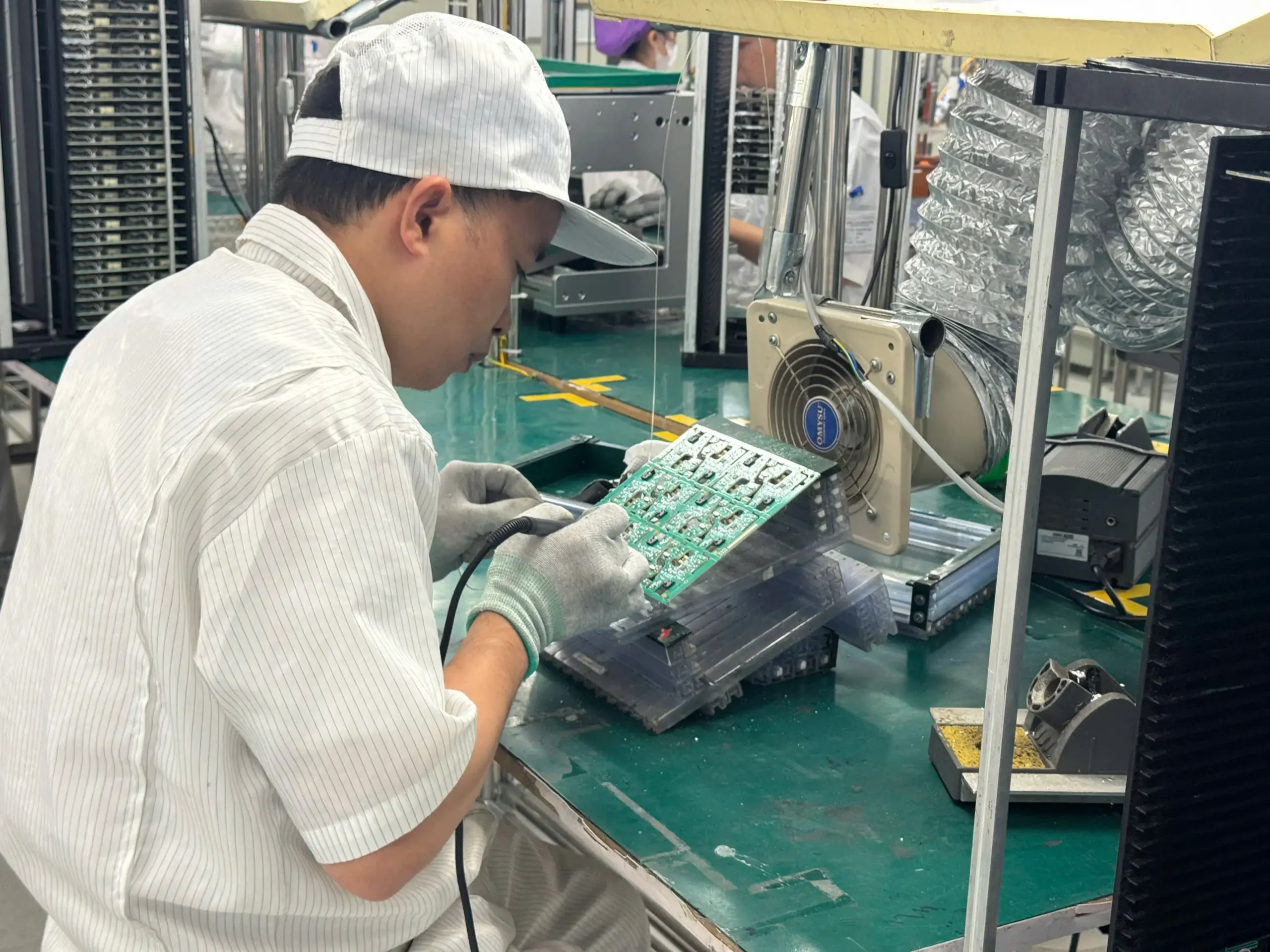
3. Through-Hole Assembly (THT / DIP)
Through-hole assembly is typically used when higher mechanical strength or power handling capability is required.
This method is commonly applied to:
-
High-power components
-
Connectors and transformers
-
Components subject to mechanical stress
Through-hole components may be assembled using:
-
Wave soldering for high-volume production
-
Manual soldering for prototypes or low-volume builds
In many designs, SMT and THT processes are combined to achieve both compact layout and mechanical durability.
4. Soldering Quality & Cleaning
Proper soldering techniques are critical to ensuring stable electrical connections and long-term reliability.
After soldering, boards may undergo:
-
Visual inspection
-
Flux residue cleaning using specialized solvents or deionized water systems
Effective cleaning helps:
-
Prevent corrosion
-
Reduce leakage currents
-
Improve long-term performance in harsh or high-humidity environments
Why a Controlled PCBA Process Matters
Each step in the PCBA assembly process contributes directly to:
-
Product quality and reliability
-
Manufacturing yield
-
Compliance with industry standards
-
Customer satisfaction and field performance
Professional PCBA manufacturers follow strict process controls, inspection procedures, and quality management systems to ensure consistent results across prototype, low-volume, and mass production.
PCBA Testing and inspection methods
In electronics manufacturing, PCBA testing and inspection play a critical role in ensuring product quality, operational stability, and long-term reliability. Even minor soldering defects or incorrect component placement can lead to high failure rates, field issues, and significant cost losses.
Professional PCBA manufacturers implement multiple inspection and testing methods throughout the production process to detect defects early and ensure that assembled boards meet both technical specifications and real-world application requirements.
1. AOI (Automated Optical Inspection)
AOI is the most widely used inspection method in modern SMT production lines. High-resolution cameras automatically capture images of the assembled PCB and compare them against reference data to identify defects.
AOI can detect:
-
Missing or incorrect components
-
Misaligned or rotated components
-
Soldering defects such as insufficient solder, excess solder, or solder bridges
-
Printing or placement inaccuracies
Key advantages of AOI:
-
High inspection speed suitable for mass production
-
Early defect detection immediately after SMT processes
-
Reduced reliance on manual visual inspection
AOI is typically performed after solder paste printing and reflow soldering to ensure consistent quality control.
2. X-Ray Inspection – Detecting Hidden Solder Joints
X-ray inspection is used to examine solder joints that are not visible to the naked eye or AOI systems, especially in complex component packages.
This method is essential for:
-
BGA (Ball Grid Array)
-
QFN, LGA, and other high-density packages
-
Multi-pin and fine-pitch components
X-ray inspection can reveal:
-
Voids within solder joints
-
Open or incomplete solder connections
-
Internal solder bridges
-
BGA ball misalignment
For high-reliability applications such as medical devices, industrial electronics, and automotive systems, X-ray inspection is often mandatory.
3. ICT (In-Circuit Testing)
In-Circuit Testing (ICT) electrically tests individual components and circuits on a fully assembled PCBA using probes or a bed-of-nails fixture.
ICT enables manufacturers to:
-
Detect open and short circuits
-
Measure component values (resistors, capacitors, inductors)
-
Identify incorrect or faulty components
-
Verify solder joint integrity at the electrical level
Benefits of ICT include:
-
High accuracy and repeatability
-
Early detection of electrical defects
-
Suitability for medium- to high-volume production
ICT is most effective when combined with proper DFT (Design for Testability) considerations.
4. Functional Testing (FCT)
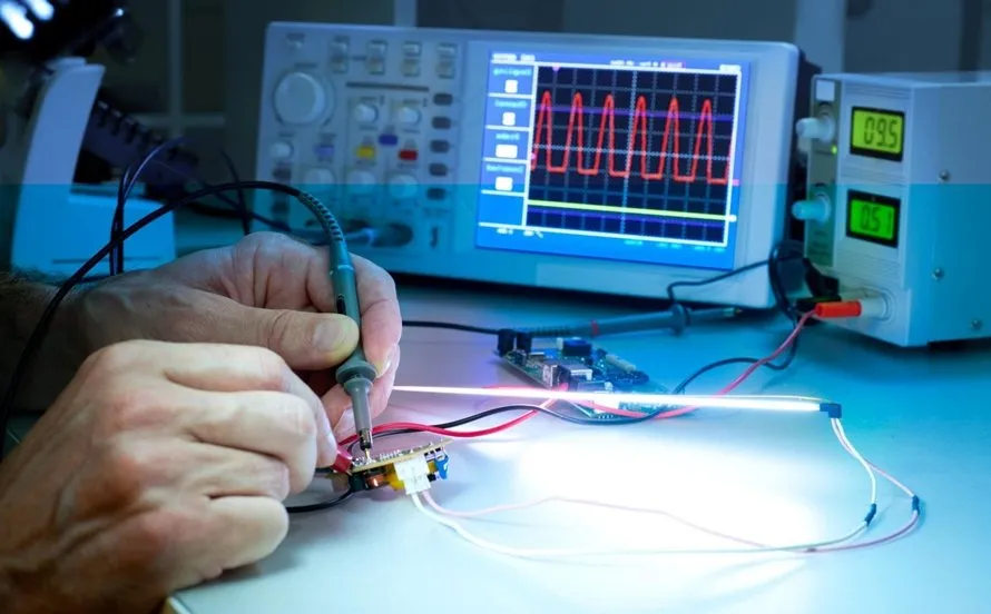
Functional Circuit Testing (FCT) is the final validation step that confirms whether the PCBA operates correctly according to its intended design and application.
Rather than testing individual components, FCT simulates real operating conditions, including:
-
Power-up and current/voltage measurement
-
Input/output signal verification
-
Communication interface testing (UART, CAN, I2C, SPI, etc.)
-
Control logic and system response validation
Why FCT matters:
-
Ensures the PCBA is ready for direct integration into the final product
-
Reduces risks during box-build assembly
-
Improves field reliability and end-user satisfaction
FCT is essential for commercial and mass-produced PCBA products.
Effective PCBA Testing Strategy
An optimized PCBA testing strategy typically combines:
-
AOI and X-ray inspection for solder joint quality
-
ICT for electrical integrity and component validation
-
FCT for full functional verification
This multi-layered approach helps:
-
Detect defects at early stages
-
Minimize rework and repair costs
-
Improve production yield
-
Ensure consistent quality across production batches
Applications of PCBA in modern electronics manufacturing
PCBA (Printed Circuit Board Assembly) is a core building block of almost all electronic products today. Thanks to its high level of integration, reliability, and application-specific customization, PCBA is widely used across multiple industries.
1. Consumer electronics
In the consumer electronics sector, PCBA is found in products such as:
-
Smartphones
-
Wearable devices (smartwatches, fitness trackers)
-
TVs, audio equipment, and smart home appliances
This industry requires PCBA solutions that offer:
-
Compact size and high component density
-
Cost efficiency for high-volume production
-
Stable performance in everyday usage environments
2. Automotive electronics
PCBA plays a critical role in modern automotive electronics, including:
-
ADAS (Advanced Driver Assistance Systems)
-
In-vehicle infotainment systems
-
Engine control units, battery management, and sensor modules
Automotive PCBA requires:
-
High reliability and long service life
-
Resistance to vibration, temperature extremes, and harsh environments
-
Compliance with strict automotive safety and quality standards
3. Medical devices
In the medical device industry, PCBA is used in:
-
Patient monitoring equipment
-
Diagnostic and laboratory devices
-
Therapeutic and healthcare support systems
Medical PCBA demands:
-
Extremely high accuracy and operational stability
-
Clear traceability and rigorous quality control
-
Compliance with stringent regulatory and industry standards
4. Industrial automation
PCBA serves as the central electronic component in:
-
PLCs and industrial controllers
-
Power supplies and variable frequency drives
-
Robotics and automated production lines
Key requirements in this sector include:
-
Continuous 24/7 operation
-
High durability in industrial environments
-
Long product lifecycle and ease of maintenance
5. IoT and smart devices
In the IoT and smart device ecosystem, PCBA is widely applied in:
-
Smart home systems
-
Environmental sensors
-
Wireless communication and remote monitoring devices
Typical PCBA requirements for IoT applications:
-
Low power consumption
-
Compact and flexible design
-
Support for multiple connectivity protocols (Wi-Fi, Bluetooth, LoRa, NB-IoT, etc.)
Each PCBA application sector has its own specific requirements for quality, reliability, and regulatory compliance, making the selection of a qualified PCBA manufacturer essential.
Key factors affecting PCBA cost
PCBA manufacturing cost varies significantly depending on technical complexity and production scale.
1. Number and type of components
-
Standard vs. specialized components
-
Surface-mount (SMD) vs. through-hole (THT) components
-
Component availability and sourcing difficulty
2. Assembly technology
-
SMT-only assembly typically results in lower costs
-
Mixed SMT + THT assembly adds process complexity and cost
3. PCB layer count
-
Multi-layer PCBs increase fabrication and assembly costs
-
Complex designs require stricter process control
4. Testing and inspection requirements
-
AOI, X-ray, ICT, and FCT
-
Higher testing coverage increases cost but significantly improves reliability
5. Production volume
-
Prototype and NPI builds have higher unit costs
-
Mass production enables cost optimization through economies of scale
Understanding these cost drivers allows businesses to optimize PCBA expenses while maintaining product quality and reliability.
Common PCBA defects and how to prevent them
During PCBA manufacturing, several common defects can negatively impact product performance and reliability.
Common PCBA defects include
-
Cold solder joints resulting in unstable electrical connections
-
Tombstoning, where SMD components stand upright due to uneven soldering forces
-
Short circuits caused by solder bridges or excess solder
-
Missing or incorrect components
Effective prevention methods
-
Apply DFM (Design for Manufacturability) principles early in the design stage
-
Maintain strict control over solder paste printing and reflow profiles
-
Use appropriate inspection methods such as AOI and X-ray
-
Standardize manufacturing processes and continuously train technical staff
Preventing defects at the design and process level is far more effective than correcting issues after production.
SHDC – Leading PCBA Manufacturer in Vietnam
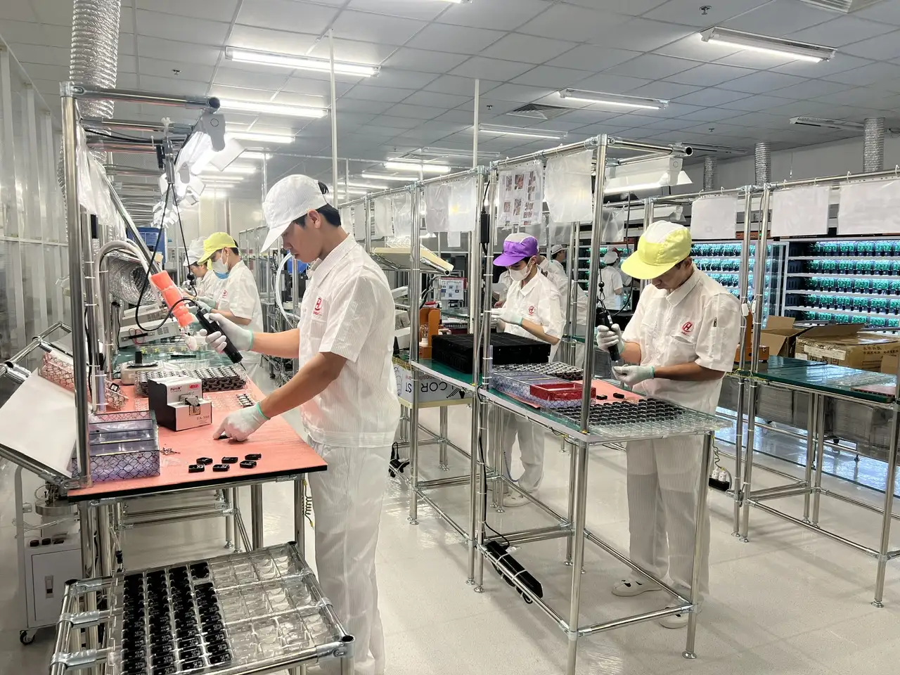
SHDC Electronics Co., Ltd. is a member of NAHACO Group, a 100% Vietnamese-owned enterprise, specializing in PCBA manufacturing and SMT assembly services in Vietnam. Our manufacturing facility is located at Factory A1-2, Lot 5, VSIP Hai Duong Industrial Park, Cam Dien Commune, Cam Giang District, Hai Duong Province, one of the most developed industrial zones in Northern Vietnam.
As one of the pioneering Vietnamese companies in PCBA assembly, SHDC provides end-to-end electronics manufacturing services, including SMT assembly, through-hole assembly (THT/DIP), functional testing, and mass production. We also manufacture power adapters, chargers, and electronic devices for export markets, meeting international quality and compliance standards.
In addition to OEM/ODM PCBA services, SHDC owns its own consumer electronics brand, Winsler, with a clear mission: delivering high-quality “Made in Vietnam” electronic products, designed, manufactured, and branded by a Vietnamese company for both domestic and global markets.
Experienced team & international standards
SHDC is backed by a highly experienced engineering and production team with extensive expertise in PCB assembly and electronics manufacturing. Our management team has previously held senior leadership positions at multinational electronics corporations, ensuring professional manufacturing management, strict process control, and global-standard execution.
Quality commitment & manufacturing capability
We are committed to delivering:
-
High-reliability PCBA products
-
Clear material traceability and origin control
-
Competitive manufacturing costs
-
Stable lead time for prototype, low-volume, and mass production
By strictly following IPC standards, ISO-compliant quality systems, and comprehensive testing procedures, SHDC ensures consistent product quality, long-term reliability, and scalable manufacturing capacity for global B2B customers.
Your trusted PCBA assembly partner in Vietnam
With modern SMT production lines, rigorous quality control, and a customer-oriented approach, SHDC is your trusted PCBA manufacturer and SMT assembly partner in Vietnam, supporting projects across industrial electronics, power supplies, IoT devices, and consumer electronics.
Conclusion
Understanding the PCBA assembly process, testing methods, applications, and cost drivers enables businesses and engineers to make more accurate and effective manufacturing decisions. For electronics projects that require high stability and quality, choosing a trusted PCBA assembly partner such as SHDC helps companies control technical risks, ensure production schedules, and optimize overall investment efficiency.
FQAs
Q1: What PCBA services does SHDC provide?
A: SHDC provides one-stop PCBA services including SMT assembly, THT/DIP assembly, functional testing, and mass production.
Q2: Does SHDC support OEM and ODM projects?
A: Yes, SHDC offers flexible OEM and ODM PCBA manufacturing solutions for global customers.
Q3: What industries does SHDC serve?
A: We serve industrial electronics, power supply, IoT devices, consumer electronics, and medical equipment sectors.
Q4: Can SHDC handle prototype and low-volume production?
A: Yes, we support prototype, low-volume, and high-volume PCBA production with stable quality and lead time.
Q5: What quality standards does SHDC follow?
A: SHDC follows IPC standards and ISO-compliant quality management systems to ensure reliable PCBA performance.
Q6: Where is SHDC’s PCBA factory located?
A: Our factory is located in VSIP Hai Duong Industrial Park, Vietnam.