Tiếng Việt
 日本語
日本語If you’ve ever wondered how circuit boards are manufactured, the answer lies in a highly controlled engineering process that integrates materials science, precision fabrication, automated assembly, and rigorous quality verification.
From initial schematic design to final functional testing, modern PCB manufacturing follows a structured production lifecycle engineered to ensure electrical integrity, mechanical durability, and long-term field reliability. In this guide, we examine each stage of that lifecycle and explain how today’s manufacturing systems deliver consistent, scalable electronic production.
What Is a Circuit Boards Manufactured?
A circuit board—more formally known as a printed circuit board (PCB)—is the foundational platform that mechanically supports and electrically connects electronic components. Copper traces embedded within insulating substrate layers form conductive pathways that replace traditional point-to-point wiring.
PCBs can range from:
-
Simple single-layer boards used in basic consumer electronics
-
Multilayer boards found in industrial control systems
-
High-density interconnect (HDI) designs used in advanced computing and telecommunications
Regardless of complexity, the manufacturing lifecycle follows a structured sequence of design, fabrication, assembly, and testing.
How Are Circuit Boards Manufactured?
Step 1: PCB Design and Engineering Preparation
Before any physical manufacturing begins, PCB production starts with engineering design.
Schematic Design
Electrical engineers first create a schematic diagram defining component connectivity. This logical representation establishes how current flows through the system.
PCB Layout
Next, designers convert the schematic into a physical layout using EDA (Electronic Design Automation) software. This stage determines:
-
Trace routing
-
Layer stack-up configuration
-
Via placement
-
Component positioning
-
Controlled impedance requirements
Gerber File Generation
Once finalized, the design is exported into manufacturing data files (typically Gerber files). These files contain the precise geometric data needed to fabricate the board.
Design for Manufacturability (DFM)
Modern PCB production includes Design for Manufacturability (DFM) analysis. DFM ensures that:
-
Trace widths meet fabrication tolerances
-
Via aspect ratios are achievable
-
Layer stack-ups align with material availability
-
Thermal constraints are addressed
Engineering validation at this stage prevents costly redesign cycles later in production.
Step 2: PCB Fabrication — Manufacturing the Bare Board
The fabrication stage transforms raw materials into a functional bare PCB without components.
Material Preparation
Most PCBs use FR-4 laminate, a fiberglass-reinforced epoxy substrate. Sheets are clad with copper foil on one or both sides. For high-performance applications, alternative materials such as high-Tg laminates or RF substrates may be used.
Inner Layer Imaging and Etching
For multilayer boards:
-
A photoresist layer is applied to the copper surface.
-
Ultraviolet light transfers the circuit pattern onto the panel.
-
Chemical etching removes unwanted copper.
This process creates the conductive pathways that will later connect components.
Precision during imaging and etching directly affects signal integrity and current-carrying capacity.
Layer Lamination
Multilayer PCBs are created by stacking inner layers with prepreg (resin-impregnated fiberglass) and bonding them under heat and pressure in a lamination press.
Uniform temperature and pressure control are essential to prevent delamination or layer misalignment.
Drilling and Via Formation
After lamination, CNC drilling machines create holes for:
-
Through-hole component leads
-
Mechanical mounting
-
Electrical interconnections (vias)
For advanced HDI boards, laser drilling forms microvias that connect closely spaced layers.
Copper Plating
The drilled holes are plated with copper to create conductive connections between layers. This electroplating process must maintain strict thickness control to ensure structural reliability.
Outer Layer Imaging and Etching
The outer circuit layers undergo a similar imaging and etching process to define final routing patterns.
Solder Mask and Silkscreen
A protective solder mask coating is applied to prevent oxidation and unintended solder bridging. Silkscreen markings are added to label components and reference points.
Surface Finishing
Surface finishes protect exposed copper pads and improve solderability. Common finishes include:
-
ENIG (Electroless Nickel Immersion Gold)
-
HASL (Hot Air Solder Leveling)
-
OSP (Organic Solderability Preservative)
Each finish serves different cost and performance requirements.
Electrical Testing
Before shipment, bare boards undergo electrical testing to verify continuity and isolation. Automated systems detect short circuits or open connections.
At this stage, the PCB fabrication process is complete—but the board is not yet functional.
>>> Read more: How to Evaluate a PCB Fabrication Factory
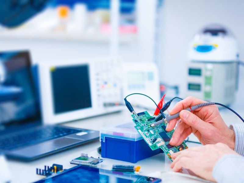
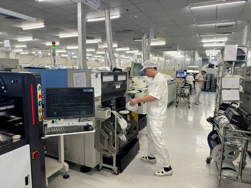
Step 3: PCB Assembly — Adding Electronic Components
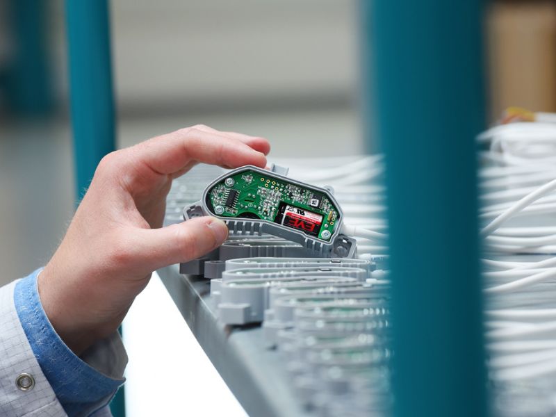
PCB assembly (PCBA) transforms the bare board into a functional electronic system.
Solder Paste Application
A stencil printer deposits solder paste onto component pads. Paste volume control is critical for reliable solder joints.
Surface Mount Technology (SMT) Placement
Automated pick-and-place machines position surface-mount components at high speed and precision. Modern systems can place thousands of components per hour with micron-level accuracy.
Reflow Soldering
Boards pass through a reflow oven where controlled temperature profiles melt solder paste and form permanent joints.
Thermal profiling ensures proper wetting without damaging sensitive components.
Through-Hole Insertion and Wave Soldering
Components with leads inserted through drilled holes are soldered using wave soldering or selective soldering systems.
Inspection and X-Ray Analysis
Quality inspection includes:
-
Automated Optical Inspection (AOI)
-
3D solder paste inspection (SPI)
-
X-ray inspection for hidden joints such as BGAs
Inspection systems detect alignment errors, insufficient solder, and bridging defects.
Step 4: Testing and Quality Assurance
Modern PCB manufacturing emphasizes verification before product release.
In-Circuit Testing (ICT)
ICT checks individual circuit nodes for proper electrical behavior.
Functional Testing (FCT)
Functional testing simulates real-world operating conditions to confirm system performance.
Environmental and Reliability Testing
In certain industries, boards undergo:
-
Thermal cycling
-
Vibration testing
-
Burn-in testing
These procedures validate durability under harsh conditions.
How Modern PCB Manufacturing Has Evolved
PCB production has advanced significantly over the past two decades.
Increased Automation
Robotics and automated inspection systems reduce human error and improve repeatability.
High-Density Interconnect (HDI)
Laser-drilled microvias enable compact, multilayer designs supporting advanced electronics.
Fine-Pitch Component Support
Modern SMT lines handle components as small as 0201, requiring extremely precise placement capability.
Digital Production Systems
Integrated ERP (Enterprise Resource Planning) and MES (Manufacturing Execution Systems) platforms track:
-
Material traceability
-
Production scheduling
-
Process data
-
Quality metrics
Digitalization improves transparency and scalability.
Manufacturers such as SHDC Electronic Company Limited, operating within structured industrial facilities in Southeast Asia, illustrate this system-driven approach. By integrating ISO-certified quality management systems with ERP, MES, and advanced SMT inspection infrastructure, facilities like SHDC reflect the global shift toward digitally controlled electronics manufacturing environments serving international OEM requirements.
This evolution demonstrates that modern PCB production is no longer a purely mechanical activity—it is an engineering-managed, data-driven process.
Where Are Circuit Boards Manufactured Today?
PCB production is globally distributed.
-
The United States maintains specialized high-reliability manufacturing.
-
China remains a dominant high-volume producer.
-
Southeast Asia has emerged as a strategic manufacturing hub due to cost efficiency, skilled labor, and industrial infrastructure.
-
Mexico supports nearshore production for North American supply chains.
Supplier selection often balances cost, capability, certification, and geopolitical risk considerations.
Frequently Asked Questions
How long does it take to manufacture a PCB?
Prototype fabrication may take several days, while volume production timelines vary depending on complexity and capacity.
What materials are used in circuit boards?
Most boards use FR-4 laminate with copper foil, though specialized materials support high-frequency or high-temperature applications.
What is the difference between PCB fabrication and assembly?
Fabrication produces the bare board structure. Assembly installs electronic components and performs soldering and testing.
Are circuit boards still made in the USA?
Yes, especially for defense, aerospace, and high-reliability sectors, though global production networks are common.
Conclusion
So, how are circuit boards manufactured? The process begins with engineering design, progresses through precision fabrication of copper-clad laminates, continues with automated component assembly, and concludes with rigorous inspection and testing.
Modern PCB production integrates materials science, robotics, quality management systems, and digital manufacturing infrastructure to ensure repeatable, scalable results. As electronic devices grow more compact and complex, the discipline of circuit board manufacturing continues to evolve—driven by automation, high-density design, and data-driven process control.
Understanding this lifecycle not only clarifies how electronic devices are built—it reveals why manufacturing maturity and engineering oversight are essential to delivering reliable electronics in today’s global market.