Tiếng Việt
 日本語
日本語In modern PCB assembly, soldering is not just a process step—it directly impacts yield, reliability, and cost. Among the most widely used methods, wave soldering and reflow soldering serve different purposes and are often misunderstood. For OEMs and engineers, choosing the right method is less about preference and more about design compatibility, production scale, and long-term reliability. This article compares wave soldering and reflow soldering to help businesses choose the solution that best fits their production needs
What Is Wave Soldering?
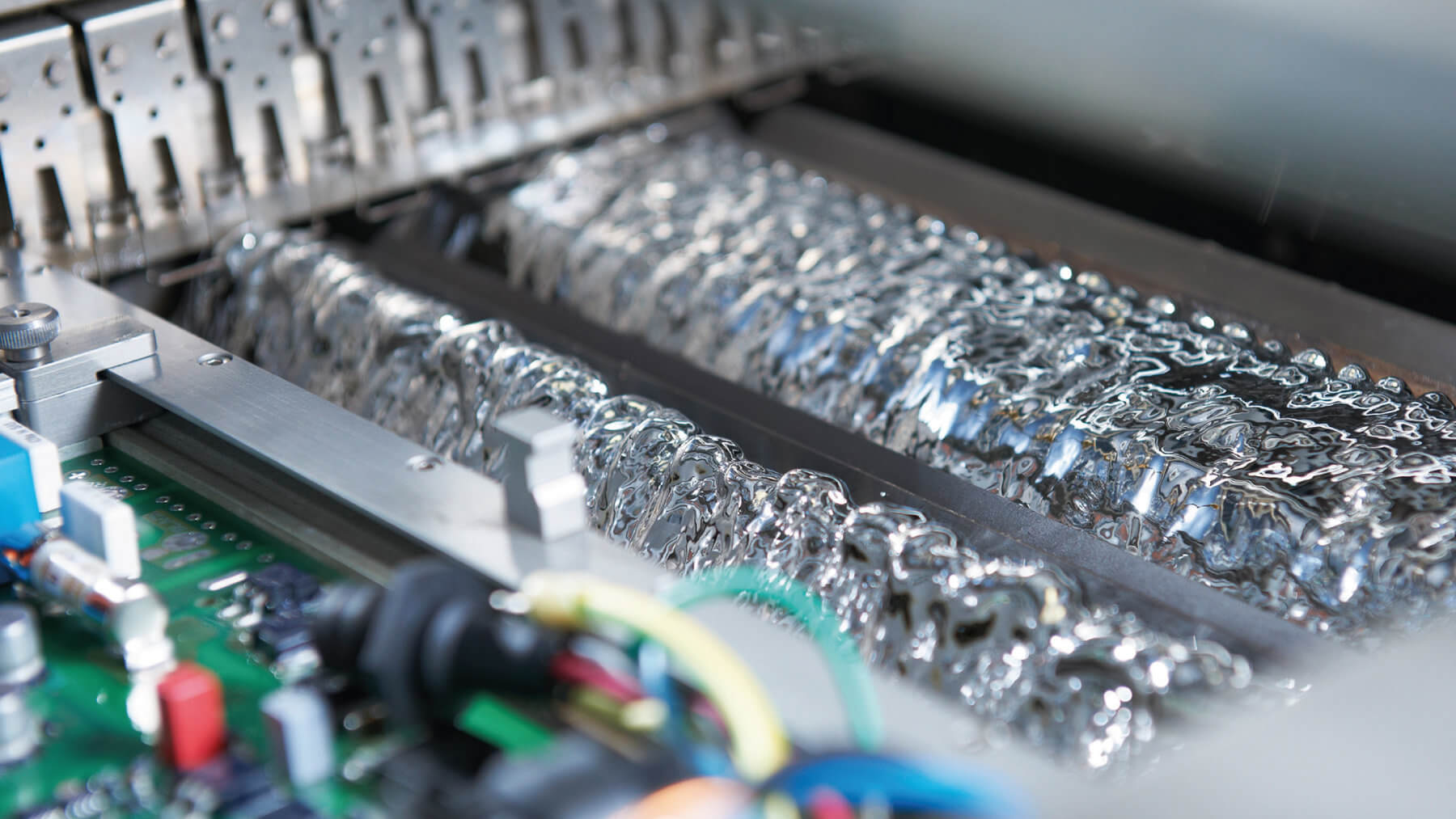
Wave soldering is a process primarily used for through-hole (THT) components, where the PCB passes over a molten wave of solder to create joints.
How it works:
- Components are inserted into drilled holes
- Flux is applied to prepare surfaces
- The board passes over a wave of molten solder
- Solder fills the holes and forms joints
Where it fits:
- Through-hole components (connectors, transformers, large capacitors)
- Mixed-technology boards (SMT + THT)
- High-volume production environments
Strengths:
- Efficient for bulk soldering of THT components
- Strong mechanical joints
- Suitable for rugged applications
Limitations:
- Less precise than SMT processes
- Not ideal for high-density designs
- Risk of defects like bridging if not controlled properly
What Is Reflow Soldering?
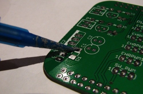
Reflow soldering is the standard method for surface-mount technology (SMT), used in most modern electronics.
How it works:
- Solder paste is printed onto PCB pads
- Components are placed using pick-and-place machines
- The board passes through a reflow oven
- Heat melts the solder paste to form joints
Where it fits:
- High-density PCB designs
- Miniaturized electronics
- Fully automated SMT lines
Strengths:
- High precision and repeatability
- Ideal for complex, high-speed production
- Supports fine-pitch and BGA components
Limitations:
- Requires precise thermal profiles
- Sensitive to process variation
- Defects like tombstoning or voiding can occur
Wave Soldering vs Reflow Soldering: Key Differences
| Factor | Wave Soldering | Reflow Soldering |
|---|---|---|
| Component Type | Through-hole (THT) | Surface-mount (SMT) |
| Process Method | Molten solder wave | Controlled heating in oven |
| Precision | Moderate | High |
| Production Speed | High for THT | High for SMT automation |
| Cost Efficiency | Best for THT volume | Best for SMT volume |
| Defect Risk | Bridging, insufficient fill | Tombstoning, voiding |
Key takeaway: Wave soldering and reflow soldering are not interchangeable—they are complementary processes designed for different component technologies.
>>>Read more: Domestic vs Offshore PCB Assembly: Which Manufacturing Option Is Right for Your Business?
When to Use Wave Soldering
Wave soldering remains essential in scenarios where mechanical strength and through-hole design are critical.
Use wave soldering when:
- Your PCB includes through-hole components
- You require strong mechanical connections
- You are running high-volume THT production
- Your design includes connectors or power components
Practical advantages:
- Fast processing for large batches
- Reliable solder joints for heavy components
- Cost-effective for THT-heavy designs
Constraints to consider:
- Limited suitability for dense SMT layouts
- Requires careful masking in mixed assemblies
- Higher risk of solder bridging without optimization
When to Use Reflow Soldering
Reflow soldering dominates modern electronics because of its compatibility with miniaturization and automation.
Use reflow soldering when:
- Your design is SMT-based
- You require high-density layouts
- Your production involves automated SMT lines
- You need consistent, repeatable quality
Practical advantages:
- High accuracy for small components
- Scalable for mass production
- Supports complex packages (QFN, BGA)
Constraints to consider:
- Requires tight process control
- Sensitive to solder paste quality and stencil design
- Thermal stress must be managed carefully
>>>Read more: PCB Assembly Cost: How Much Does It Cost in 2026? (Full Breakdown)
Wave vs Reflow in Modern PCB Assembly Lines
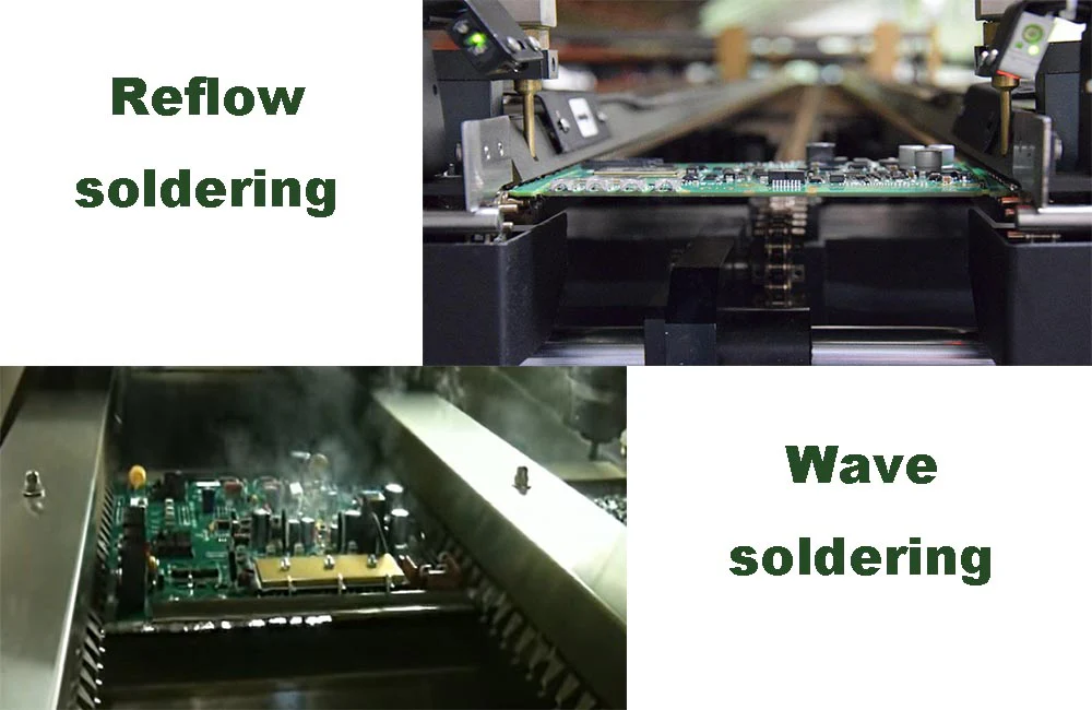
In real-world manufacturing, the choice is rarely “wave vs reflow.” Most production environments use a hybrid approach.
Typical workflow:
- SMT components assembled using reflow soldering
- Through-hole components added
- Wave soldering or selective soldering applied
Why this matters:
- Modern boards often combine SMT and THT
- Each process handles what it does best
- Integration improves overall efficiency
Insight: Reflow is the backbone of modern PCB assembly, while wave soldering plays a supporting but critical role.
Common Soldering Defects and How to Avoid Them
Understanding defects is essential for improving yield and reliability.
In wave soldering:
- Solder bridging → caused by excess solder or poor design spacing
- Insufficient hole fill → due to poor wetting or incorrect parameters
In reflow soldering:
- Tombstoning → uneven heating causes components to lift
- Voiding → trapped gases reduce joint reliability
- Cold joints → improper temperature profile
Prevention strategies:
- Optimize PCB design (DFM)
- Control process parameters
- Use proper inspection (AOI, X-ray)
- Maintain consistent materials and profiles
Defect control is not just a quality issue—it directly impacts cost and production efficiency.
How Soldering Method Affects PCB Assembly Cost and Yield
The choice between wave and reflow soldering influences both cost structure and yield performance.
Cost perspective:
- Reflow = higher equipment cost but lower labor per unit
- Wave = efficient for bulk THT but requires setup and control
Yield perspective:
- Reflow → higher consistency in automated lines
- Wave → dependent on process tuning and board design
Hidden cost factors:
- Rework due to defects
- Scrap from poor yield
- Delays caused by process instability
Key insight: The most cost-effective method is not the cheapest—it’s the one that delivers stable yield at scale.
>>>Read more: PCB Prototyping Services Cost: What Affects Your Prototype Price?
Choosing the Right Process for Your PCB Assembly Project
There is no universally “better” method. The right choice depends on:
- PCB design (SMT vs THT)
- Component types
- Production volume
- Reliability requirements
Decision framework:
- SMT-heavy design → reflow soldering
- THT-heavy design → wave soldering
- Mixed design → hybrid approach
OEMs that align process selection with design early avoid costly adjustments later.
How a Modern EMS Provider Optimizes Both Processes
Efficient PCB assembly requires more than selecting a process—it requires integrating processes into a controlled system.
A capable EMS provider will:
- Align DFM with soldering methods
- Optimize SMT and THT workflows
- Control process parameters for consistent yield
- Implement multi-stage inspection
This integrated approach reduces:
- defects
- rework
- production delays
Integrated SMT and Wave Soldering in High-Volume Production

In scalable manufacturing environments, combining SMT and wave soldering effectively is critical for maintaining quality and efficiency.
At SHDC, PCB assembly programs are structured to support both processes within a unified production system.
This includes:
- Multiple SMT lines with controlled reflow profiles
- Dedicated wave soldering systems for through-hole assembly
- Integrated inspection processes (AOI, ICT, functional testing)
- Process alignment between SMT and DIP stages
By coordinating these processes within a single workflow, manufacturers can:
- Improve yield stability
- Reduce defect rates
- Maintain consistent quality across production volumes
For OEMs scaling production, this level of integration is often the difference between stable output and costly variability.
FAQs
– What is the main difference between wave soldering and reflow soldering?
Wave soldering is used for through-hole components, while reflow soldering is used for surface-mount components.
– Which is better: wave or reflow soldering?
Neither is universally better. Each is suited for different component types and design requirements.
– Can wave soldering be used for SMT components?
Not typically. SMT components are best handled with reflow soldering.
– Why is reflow soldering more common today?
Because modern electronics rely heavily on SMT and high-density PCB designs.
– What defects are common in these processes?
Wave soldering often faces bridging and fill issues, while reflow soldering can have tombstoning and voiding defects.
Final Thoughts
Wave soldering vs reflow soldering are not competing technologies—they are complementary tools in PCB assembly. Understanding their differences—and more importantly, when to use each—allows OEMs to optimize production for cost, quality, and scalability. In modern electronics manufacturing, success doesn’t come from choosing one process over the other. It comes from integrating both effectively within a well-controlled production system.
>>>Read more: PCB Board Fabrication vs PCB Assembly: What OEMs Need to Know Before Production