Tiếng Việt
 日本語
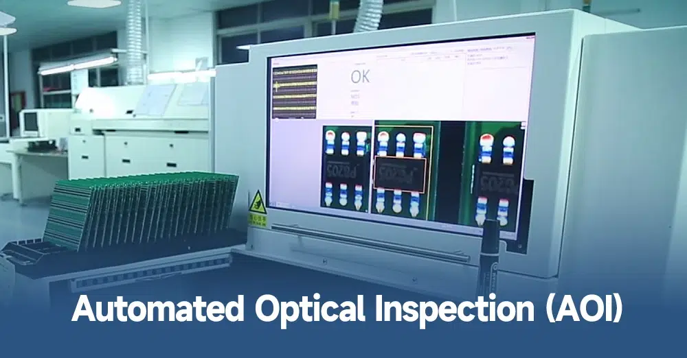
日本語In modern electronics manufacturing, ensuring product quality is critical—especially in PCB assembly, where even small defects can lead to costly failures. One of the most widely used technologies for quality control is Automated Optical Inspection (AOI). AOI systems use advanced cameras and software to automatically detect defects on printed circuit boards, helping manufacturers maintain consistency, reduce errors, and improve reliability. In this guide, you’ll learn how AOI works, what defects it detects, and why it plays a key role in PCB assembly quality.
What Is Automated Optical Inspection (AOI)?
Definition of AOI in Electronics Manufacturing
Automated Optical Inspection (AOI) is a non-contact inspection method that uses high-resolution cameras and image processing software to detect defects in electronic assemblies. It is widely used in PCB manufacturing to ensure components are correctly placed and soldered.
Unlike manual inspection, AOI systems operate automatically, allowing manufacturers to inspect large volumes of boards quickly and consistently. This makes AOI an essential part of modern high-volume electronics production.
Why AOI Is Used in PCB Assembly
PCB assembly involves complex processes such as solder paste printing, component placement, and reflow soldering. Each step introduces potential defects that can affect product performance.
AOI is used to:
- Detect defects early in the production process
- Reduce reliance on human inspection
- Improve consistency across batches
- Lower rework and scrap costs
By identifying issues at an early stage, AOI helps manufacturers prevent defective boards from progressing further down the production line.
>>>Read more: Is AOI Enough in PCBA Testing?
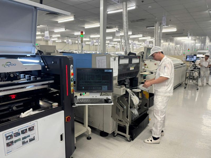
How AOI Works in PCB Assembly
Image Capture and Lighting Techniques
AOI systems rely on advanced imaging technology to capture detailed images of the PCB surface. Multiple cameras and lighting angles are used to highlight different features, such as solder joints and component edges.
Lighting plays a critical role in inspection accuracy. Techniques such as angled lighting, RGB illumination, and structured light help enhance contrast and reveal defects that may not be visible under standard lighting conditions.
Comparison with Reference Data
Once images are captured, the AOI system compares them against a predefined reference, often called a “golden board.” This reference represents a correctly assembled PCB.
The software analyzes differences between the inspected board and the reference to identify anomalies. Even small deviations in component position or solder shape can be detected.
Defect Detection Algorithms
Modern AOI systems use sophisticated algorithms to identify defects. These include rule-based systems and, increasingly, AI-driven models that improve detection accuracy over time.
These algorithms evaluate factors such as:
- Shape and size of solder joints
- Component alignment
- Color variations indicating defects
As a result, AOI systems can detect subtle issues that might be missed during manual inspection.
Inspection Stages (2D vs 3D AOI)
AOI systems are typically categorized into 2D and 3D inspection.
- 2D AOI analyzes flat images and is effective for detecting surface-level defects.
- 3D AOI uses height measurement to evaluate solder volume and joint geometry, providing more accurate inspection for complex assemblies.
3D AOI is increasingly used in high-reliability applications where precision is critical.
>>>Read more: PCBA Contract Manufacturing: What US Companies Should Know Before Outsourcing
Common PCB Defects Detected by AOI
Soldering Defects
AOI systems are highly effective at identifying solder-related issues, including:
- Cold solder joints
- Solder bridging (short circuits)
- Insufficient or excessive solder
- Voids and uneven joints
These defects can significantly impact electrical performance and long-term reliability.
Component Placement Errors
Incorrect component placement is another common issue in PCB assembly. AOI can detect:
- Missing components
- Misaligned components
- Incorrect component types
Detecting these errors early prevents functional failures and costly rework.
Polarity and Orientation Issues
Certain components, such as diodes and capacitors, must be placed with correct polarity. AOI systems verify orientation and ensure components are installed correctly.
Incorrect polarity can lead to immediate circuit failure or long-term reliability issues.
Surface and Structural Defects
AOI can also identify physical defects on the PCB surface, including:
- Scratches or damage
- Contamination
- Poor solder mask coverage
These issues may not always cause immediate failure but can affect durability over time.
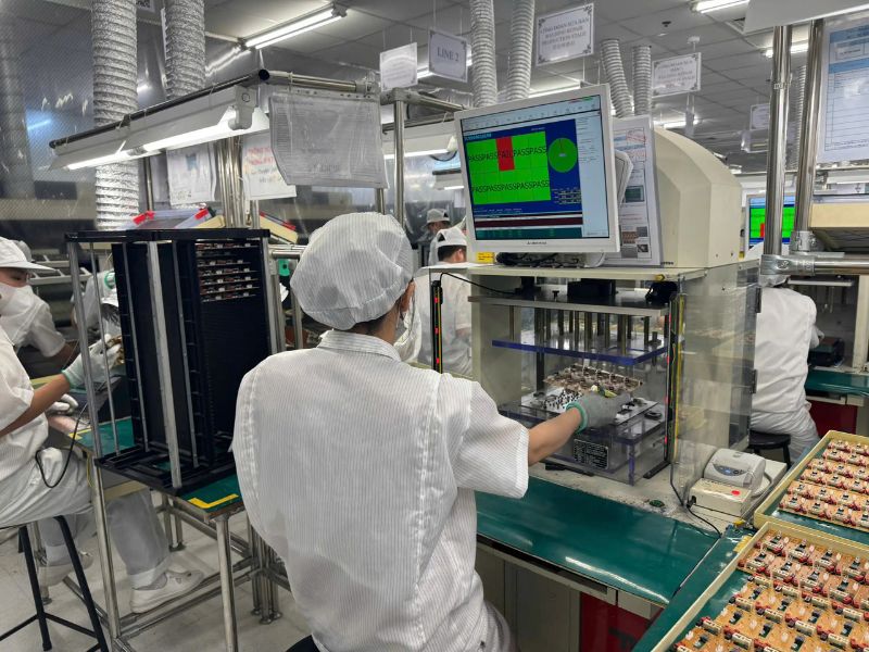
AOI in Different Stages of PCB Assembly
Pre-Reflow Inspection: Before soldering, AOI is used to inspect solder paste and component placement. This helps identify issues such as insufficient paste or misaligned components before they are permanently soldered.
Post-Reflow Inspection: After reflow soldering, AOI verifies the quality of solder joints and detects defects introduced during the heating process. This stage is critical, as it ensures that all components are properly soldered and electrically connected.
Final Quality Inspection: In the final stage, AOI serves as a last check before products move to testing or shipment. It ensures that the assembly meets quality standards and is free from visible defects.
Benefits of AOI in PCB Assembly
Improves Inspection Accuracy: AOI systems provide consistent and repeatable inspection results, reducing variability compared to manual inspection.
Reduces Human Error: Manual inspection is prone to fatigue and inconsistency. AOI eliminates these issues by automating the inspection process.
Increases Production Efficiency: AOI systems can inspect boards quickly, enabling high-speed production without compromising quality.
Enhances Product Reliability: By detecting defects early and ensuring proper assembly, AOI improves the overall reliability of electronic products.
Supports High-Volume Manufacturing: AOI is essential for scaling production, as it allows manufacturers to maintain quality while increasing output.
>>>Read more: PCB Assembly Manufacturer: How to Choose the Right Partner
AOI vs Manual Inspection in PCB Assembly
Speed and Efficiency: AOI systems can inspect hundreds of boards in the time it takes a human inspector to check a few. This makes AOI far more efficient for large-scale production.
Accuracy and Consistency: AOI provides consistent results based on predefined criteria, while manual inspection can vary between operators.
Cost Considerations: Although AOI systems require upfront investment, they reduce long-term costs by minimizing defects, rework, and returns.
AOI vs Other Inspection Methods
AOI vs Automated X-ray Inspection (AXI)
Automated X-ray Inspection (AXI) is used to inspect hidden solder joints, such as those under BGAs.
While AOI is ideal for surface inspection, AXI is necessary for detecting internal defects that cannot be seen optically.
AOI vs In-Circuit Testing (ICT)
AOI focuses on visual inspection, while ICT checks electrical performance. Both methods are complementary and often used together in PCB assembly.
How OEM Manufacturers Use AOI for Quality Control
Process Standardization: OEM manufacturers rely on AOI to standardize inspection processes across production lines, ensuring consistent quality.
Supplier Quality Assurance: AOI is often a requirement when evaluating manufacturing partners. It demonstrates the ability to maintain high inspection standards.
Compliance with IPC Standards
AOI supports compliance with standards such as:
- IPC guidelines
- IPC J-STD-001 (process control)
- IPC-A-610 (inspection criteria)
This ensures that products meet industry expectations for quality and reliability.
>>>Read more: IPC J-STD-001 vs IPC-A-610: Key Differences in PCB Assembly Standards
Best Practices for Implementing AOI in PCB Assembly
Optimize Inspection Programs: Proper programming is essential to ensure accurate defect detection and minimize false positives.
Use High-Quality Reference Data: A reliable “golden board” is critical for accurate comparison and defect identification.
Regular Calibration and Maintenance: AOI systems must be regularly calibrated to maintain accuracy and performance.
Combine AOI with Other Inspection Methods: For best results, AOI should be used alongside other inspection techniques such as AXI and functional testing.
FAQs
What is AOI used for in PCB assembly?
It is used to detect defects in soldering, component placement, and PCB surface conditions.
What defects can AOI detect?
AOI can detect solder defects, missing components, misalignment, and polarity issues.
Is AOI better than manual inspection?
AOI is faster, more consistent, and more suitable for high-volume production.
What is the difference between AOI and X-ray inspection?
AOI inspects surface features, while X-ray inspection detects hidden internal defects.
Conclusion
Automated Optical Inspection (AOI) is a critical technology in modern PCB assembly, enabling manufacturers to detect defects early and ensure consistent product quality. By combining advanced imaging with intelligent software, AOI improves efficiency, reduces errors, and enhances reliability. For OEM manufacturers, working with partners that utilize AOI is essential to achieving high-quality, dependable electronic products in today’s competitive market.
>>>Read more: High Volume PCB Assembly Services in Vietnam – Why Global Brands Choose SHDC