Tiếng Việt
 日本語
日本語The PCB manufacturing process is a precision-driven engineering discipline that directly determines the reliability, electrical performance, and long-term durability of modern electronic products. From design validation and material engineering to multilayer fabrication and final inspection, every stage must operate under strict quality control and full process traceability. Manufacturers such as SHDC, operating advanced SMT lines and integrated MES-based production systems, reflect how disciplined process control and engineering expertise are essential to meeting global OEM standards in today’s competitive electronics supply chain.
What Is PCB Manufacturing?
PCB manufacturing refers to the complete process of transforming a circuit design into a functional printed circuit board. It generally includes two major stages:
-
PCB Fabrication – Manufacturing the bare board (substrate, copper layers, vias, surface finish)
-
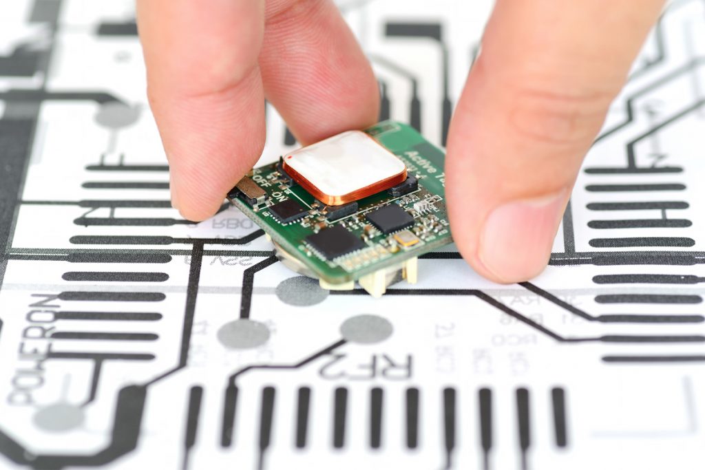
PCB Assembly (PCBA) – Mounting electronic components onto the fabricated board
In the electronics industry, these stages may be handled by separate suppliers or by a single integrated manufacturer offering full PCBA services.
PCB manufacturing applies to:
-
Single-layer boards
-
Double-layer boards
-
Multilayer PCBs
-
High-density interconnect (HDI) boards
-
Flexible PCBs (FPC)
Each type requires different materials, processing methods, and quality control standards.
>>>Read more: PCBA and PCB: A detailed technical comparison of printed circuit boards and assemblies
Overview of the PCB Manufacturing Process
The PCB manufacturing process can be divided into three high-level phases:
1. Design & Engineering Preparation
Design validation, DFM (Design for Manufacturability), and file preparation.
2. PCB Fabrication
Creating the physical bare board through imaging, etching, drilling, plating, and finishing.
3. Assembly & Testing
SMT placement, soldering, inspection, and functional verification.
Let’s examine each stage in detail.
Step-by-Step PCB Manufacturing Process
1. PCB Design and Gerber File Preparation
Every PCB begins with a CAD design created using tools such as Altium Designer, Eagle, or KiCad.
The design engineer defines:
-
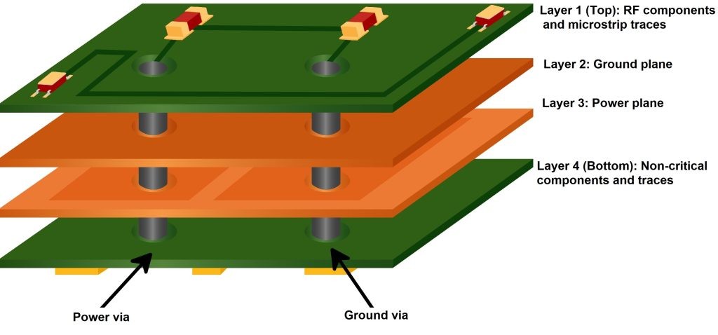
Layer stack-up
-
Trace width and spacing
-
Via structures
-
Component footprint layout
-
Power and ground planes
Once finalized, the design files are exported in Gerber format, which acts as the manufacturing blueprint.
Before production begins, manufacturers perform:
-
DFM review
-
Stack-up validation
-
Tolerance checks
-
Impedance control verification
Engineering validation at this stage prevents costly production errors.
2. Material Selection
Most standard PCBs use FR-4, a glass-reinforced epoxy laminate. However, depending on performance requirements, other materials may be selected:
-
High-Tg materials for thermal stability
-
Rogers materials for high-frequency applications
-
Polyimide for flexible PCBs
Material choice directly impacts:
-
Thermal resistance
-
Signal integrity
-
Mechanical durability
-
Long-term reliability
For high-performance or industrial applications, material selection must align with IPC standards.
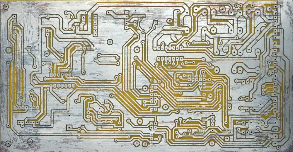
3. Inner Layer Imaging
For multilayer boards, inner copper layers are processed first.
The process includes:
-
Cleaning copper-clad laminate
-
Applying photoresist
-
UV exposure through a photomask
-
Developing the image
The exposed copper forms the circuit pattern.
Precision at this stage determines signal integrity and impedance consistency.
>>>Read more: China Alternative Electronics Manufacturing: Why Vietnam Is the Top Choice in 2026
4. Etching
Chemical etching removes unwanted copper, leaving behind only the designed trace patterns.
This step requires strict control of:
-
Chemical concentration
-
Temperature
-
Exposure duration
Improper etching can cause over-etching or under-etching, affecting conductivity and performance.
5. Layer Alignment and Lamination
For multilayer PCBs, inner layers are stacked with prepreg insulation sheets.
The stack is subjected to:
-
High temperature
-
High pressure
-
Controlled curing cycles
This lamination process permanently bonds the layers into a single rigid board.
Precise alignment is critical to ensure vias connect correctly between layers.
6. Drilling and Via Formation
After lamination, holes are drilled for:
-
Through-hole vias
-
Blind vias
-
Buried vias
-
Component mounting
Two main methods are used:
-
Mechanical drilling (standard PCBs)
-
Laser drilling (HDI boards)
Drilling accuracy directly affects electrical connectivity and reliability.
7. Copper Plating
Drilled holes are non-conductive initially. To make them electrically functional:
-
Electroless copper deposition coats the hole walls.
-
Electroplating builds up copper thickness.
This forms reliable interlayer connections.
8. Outer Layer Imaging and Etching
The outer copper layers undergo a similar imaging and etching process to form the final circuit layout.
This defines:
-
Signal traces
-
Pads
-
Ground planes
-
Power rails
9. Solder Mask Application
A solder mask layer (typically green) is applied to:
-
Protect copper traces
-
Prevent short circuits
-
Improve durability
Openings are left for component pads.
10. Silkscreen Printing
The silkscreen layer prints:
-
Component labels
-
Reference designators
-
Logos
-
Manufacturing codes
This assists assembly and service teams.
11. Surface Finishing
Surface finish protects exposed copper and improves solderability.
Common finishes include:
-
ENIG (Electroless Nickel Immersion Gold)
-
HASL (Hot Air Solder Leveling)
-
OSP (Organic Solderability Preservative)
Finish selection affects:
-
Shelf life
-
Cost
-
Solder joint reliability
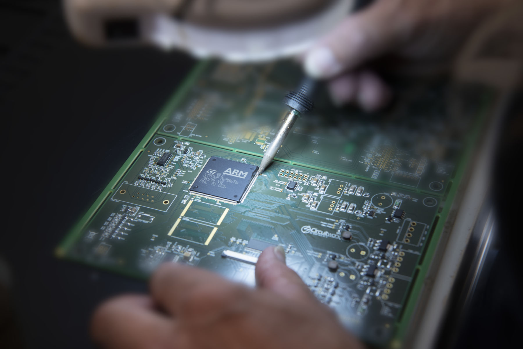
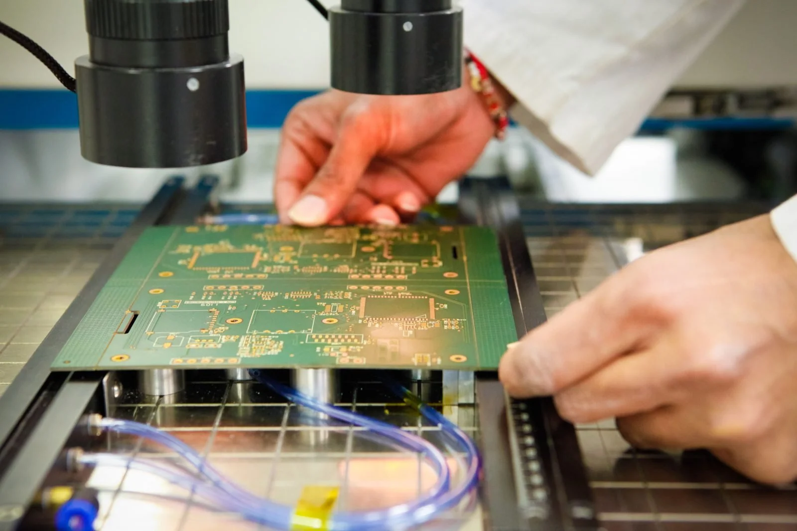
12. Electrical Testing and Final Inspection
Before shipping, boards undergo rigorous testing:
-
AOI (Automated Optical Inspection)
-
Flying probe testing
-
ICT (In-Circuit Testing)
-
FCT (Functional Circuit Testing)
This ensures:
-
No open circuits
-
No short circuits
-
Correct connectivity
High-reliability manufacturers integrate MES and quality systems to track every board batch.
How Professional PCB Manufacturers Ensure Quality
Quality control is what separates low-cost suppliers from long-term manufacturing partners.
Professional PCB manufacturers implement:
-
ISO-certified quality systems
-
Incoming Quality Control (IQC)
-
In-process Quality Control (IPQC)
-
Outgoing Quality Control (OQC)
-
MES-integrated traceability
For example, SHDC Electronic Company, located in VSIP Hai Duong Industrial Park, operates SMT production lines supported by ERP, MES, PLM, SCM, and QMS systems to maintain production transparency and traceability.
Their facility supports:
-
PCB sizes from 50×50 mm to 460×550 mm
-
Component sizes from 0201 to large-form components
-
Flexible PCB assembly (FPC)
-
3D AOI inspection systems
-
ICT and FCT functional testing
Such infrastructure ensures stable quality for international customers.
>>>Read more: Top 4 SMT Assembly Companies in Vietnam in 2026
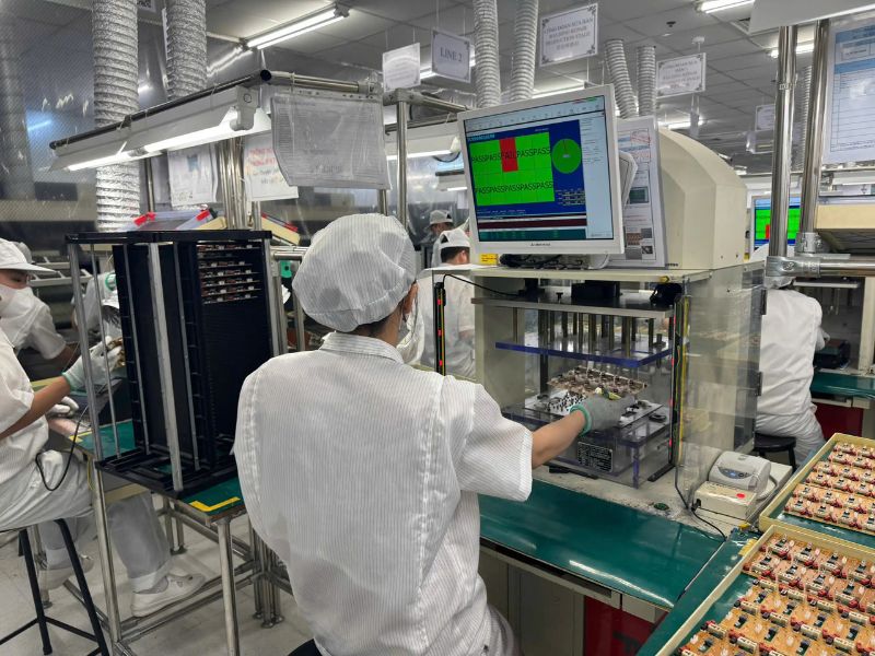
Inside a Modern PCB Manufacturing Facility
A modern PCB or PCBA facility typically includes:
-
Automated solder paste printers
-
High-speed SMT placement machines
-
Reflow ovens
-
Wave soldering machines
-
AOI 3D inspection systems
-
Functional test benches
Advanced SMT lines using Yamaha YSM series machines, combined with nitrogen reflow and automated inspection, enable consistent high-mix production.
Integrated manufacturing systems reduce:
-
Inventory waste
-
Decision time
-
Production errors
Manufacturers that combine automation with experienced engineering teams are better positioned to serve US OEMs requiring reliability and scalability.
Choosing the Right PCB Manufacturing Partner
Selecting a PCB manufacturing company involves more than comparing price quotes.
Key evaluation factors include:
1. Technical Capability
-
Multilayer capability
-
HDI experience
-
Flexible PCB support
2. Quality Certification
-
ISO certification
-
IPC compliance
3. Engineering Support
-
DFM review
-
Process optimization
-
Failure analysis support
4. Production Capacity
-
SMT line capability
-
Workforce size
-
Facility size
5. Communication & Export Experience
-
English-speaking support
-
Experience with US clients
-
Logistics capability
Manufacturers like SHDC Electronics provide full PCBA services for office equipment, consumer electronics, and industrial products, offering competitive production advantages in Asia while maintaining quality standards expected by US customers.
Frequently Asked Questions About PCB Manufacturing
How long does PCB manufacturing take?
Prototype boards may take 5–7 days. Production runs typically require 2–4 weeks depending on complexity.
What materials are used in PCB fabrication?
Common materials include FR-4, high-Tg laminates, Rogers materials, and polyimide for flexible PCBs.
What is the difference between PCB fabrication and PCB assembly?
Fabrication creates the bare board. Assembly mounts electronic components to create a functional circuit board.
What testing methods are used?
AOI, ICT, flying probe testing, and functional testing are commonly applied.
Final Thoughts
The PCB manufacturing process is a highly controlled sequence of engineering and production steps that directly determines the reliability and performance of electronic products. From design validation and copper etching to SMT placement and functional testing, every stage must meet strict quality standards.
For OEMs and product developers targeting the US market, choosing a manufacturer with technical capability, certified quality systems, and transparent production management is essential. Companies like SHDC Electronics in Vietnam demonstrate how modern PCB manufacturing integrates automation, quality control, and engineering expertise to serve global customers efficiently and competitively.