
 Tiếng Việt
 日本語
日本語
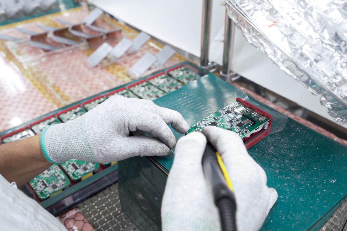
Most EMS factories will say yes to a GaN charger RFQ. Very few can actually build one to UL 62368-1 standard. The difference is not visible on a capability sheet. It comes down to three process requirements — nitrogen reflow, 3D X-ray void measurement, and 100% in-line hi-pot testing — that standard SMT shops either do not have or do not run correctly. Miss any one of them and the product fails certification, ships with a latent defect, or both. This guide breaks down exactly what GaN charger PCB assembly requires, where standard shops fall short, and why Vietnam — specifically SHDC in Hai Duong — is the only documented location outside China delivering ETL-certified GaN chargers to the US market in 2026.
Why GaN Charger PCB Assembly Is Fundamentally Different
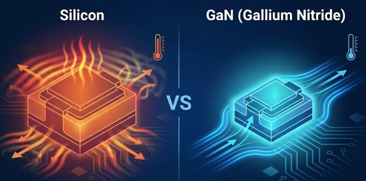
Understanding why GaN assembly is harder than standard charger assembly starts with the physics — not the marketing.
GaN vs Silicon: The Physics That Change the Process
Gallium nitride transistors switch at 100kHz–1MHz, compared to 50–100kHz for silicon MOSFETs. That higher switching frequency is what enables GaN chargers to be dramatically smaller and more efficient — but it also creates a PCB layout problem that silicon designs do not have.
At 1MHz switching, power loop inductance becomes the dominant failure mechanism. A power loop area above 0.5cm² generates enough parasitic inductance to cause voltage overshoot, ringing, and — at the certification lab — EMI emissions that fail FCC Part 15 Class B limits.
The consequence is unforgiving: one layout error means a re-spin, a new PCB fabrication cycle, and 6–8 weeks of delay before you can re-submit to the FCC lab.
The QFN Thermal Pad Problem
GaN ICs from Navitas, GaN Systems, and Infineon are packaged in QFN format — a leadless package with a thermal pad on the underside that cannot be inspected visually after reflow.
That thermal pad is the primary heat dissipation path for the GaN IC. When solder voids form beneath it during reflow, thermal resistance increases — and junction temperature rises above the rated maximum. The result is accelerated degradation and a product lifespan well below the two-year mark.
IPC-7093 sets the void threshold for QFN thermal pads at 25% maximum. Standard air reflow ovens routinely produce void percentages of 35–50% on GaN QFN packages. The only solution is nitrogen reflow — and the only way to verify it worked is 3D X-ray.
Isolation Requirements Under UL 62368-1
UL 62368-1 — the current US safety standard for audio/video and IT equipment including chargers — requires a minimum creepage distance of 6.4mm between primary (mains) and secondary (output) circuits on the PCB.
Verifying that this isolation holds under stress requires a hi-pot (dielectric withstand) test at 3000VAC minimum. This test must be performed on 100% of finished units — not a statistical sample — for US market programs. A unit that passes visual inspection but fails hi-pot is a shock hazard.
Standard SMT shops either skip hi-pot entirely or run it on a sampling basis. Neither is acceptable for a product going into US retail or enterprise channels.
The 3 Process Requirements That Separate a Real GaN Line
These three requirements are the technical gatekeepers. A factory that has all three — and can prove it with data — is a real GaN line. A factory missing any one of them is not, regardless of what their capability statement says.
Requirement 1: Nitrogen Reflow Oven
The problem: Standard reflow ovens operate in ambient air. During the reflow cycle, oxygen reacts with flux residues and solder paste, creating oxide layers that prevent complete solder wetting beneath the QFN thermal pad. The result is void formation — air pockets trapped in the solder joint.
The solution: A nitrogen reflow oven purges the reflow chamber with nitrogen gas (typically > 1000 ppm N₂ concentration), eliminating oxygen and allowing complete solder wetting. Void percentage drops from 35–50% in air reflow to below 10% in nitrogen — well within IPC-7093 limits.
How to verify: Ask the supplier for a void measurement report from a recent GaN production run, with void percentage annotated on X-ray images. A factory running nitrogen reflow has this data routinely. A factory that does not will offer a reflow profile chart instead — which measures temperature, not void.
Red flag: “We optimize our reflow profile carefully.” Profile optimization reduces void in air reflow — but cannot eliminate it. Nitrogen is the only solution.
Requirement 2: 3D X-Ray Inspection
The problem: QFN thermal pad void cannot be measured by Automated Optical Inspection (AOI), visual inspection, or 2D X-ray. 2D X-ray produces a projected image that shows void presence but cannot accurately measure void percentage — because it cannot distinguish depth.
The solution: 3D X-ray (computed tomography) reconstructs a volumetric image of the solder joint, enabling precise void percentage measurement with annotated output. This is the only method that produces IPC-7093-compliant measurement data.
How to verify: Request X-ray images with void percentage annotated from a production lot — not a sample board, a production lot. A factory with real GaN production history has this data immediately. Response time is a signal: if the data takes more than 24 hours to produce, it was not being collected routinely.
| Inspection Method | Can Detect Void | Can Measure Void % | IPC-7093 Compliant |
|---|---|---|---|
| Visual / AOI | X | X | X |
| 2D X-ray | V | V | X |
| 3D X-ray (CT) | X | X | V |
Requirement 3: 100% In-Line Hi-Pot Testing
The problem: PCB layout errors, contamination, or component placement defects can compromise the isolation barrier between primary and secondary circuits — even on boards that pass visual and AOI inspection. The only way to detect these failures is electrical stress testing.
The solution: Hi-pot testing applies 3000VAC across the primary-secondary isolation barrier for a defined dwell time (typically 1 second). Any unit with compromised isolation fails immediately. Running this test 100% in-line — on every unit, in the production flow — ensures no defective unit reaches the customer.
How to verify: Ask directly: “What percentage of finished units go through hi-pot testing, and at what voltage?” The correct answer is 100%, 3000VAC minimum. Sampling-based hi-pot — even at 10% — means 90% of units ship without isolation verification.
The liability math: A single field failure from an isolation defect in a US market product triggers CPSC reporting obligations, potential recall, and product liability exposure. 100% hi-pot testing is not a quality preference — it is a risk management requirement.
What a Standard SMT Shop Gets Wrong
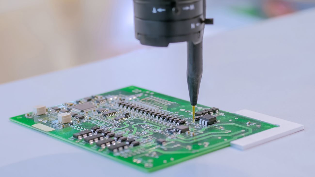
The gap between a real GaN line and a standard SMT shop is not about intent — it is about equipment and process discipline. Most standard shops genuinely believe they can build GaN chargers. Here is where the gap shows up.
The Three Most Common Failure Modes
| Failure Mode | Root Cause | Consequence |
|---|---|---|
| QFN void > 25% | No nitrogen reflow | Thermal runaway, field failure < 2 years |
| EMI fail at FCC lab | Power loop area > 0.5cm² | PCB re-spin, 6–8 week delay, re-test cost |
| Hi-pot fail at UL/ETL lab | Insufficient creepage or contamination | Re-layout, re-certify, 8–12 week delay |
All three failures are discoverable — but only at the certification lab, after tooling, after NPI investment, and after the program timeline has already been committed to a customer. Finding out at the lab costs 10–15x more than catching it in DFM review.
The DFM Review as a Capability Litmus Test
Before committing to any GaN charger PCB assembly partner, submit a Gerber package and BOM for DFM review. The quality of the feedback tells you everything about the factory’s actual GaN capability.
A real GaN factory returns a DFM report in 3–5 business days with specific comments on:
- Creepage distances between primary and secondary (minimum 6.4mm per UL 62368-1)
- GaN power loop area (target < 0.5cm²)
- Thermal via density beneath QFN pad
- PCB material specification (UL 94 V-0 required)
- Isolation boundary clearances
A factory without real GaN capability returns a report in a few hours with no issues found. The review was not performed — it was acknowledged.
This test costs nothing and eliminates the wrong partners before any financial commitment.
For a detailed breakdown of what rigorous PCB fabrication evaluation covers, see: How to Evaluate a PCB Fabrication Factory.
Why Vietnam for GaN Charger PCB Assembly in 2026
With the technical requirements established, the location question becomes straightforward: which manufacturing location outside China has the equipment stack, the certification support, and the production proof to deliver a US-market GaN charger program?
The Equipment Stack at SHDC, Hai Duong
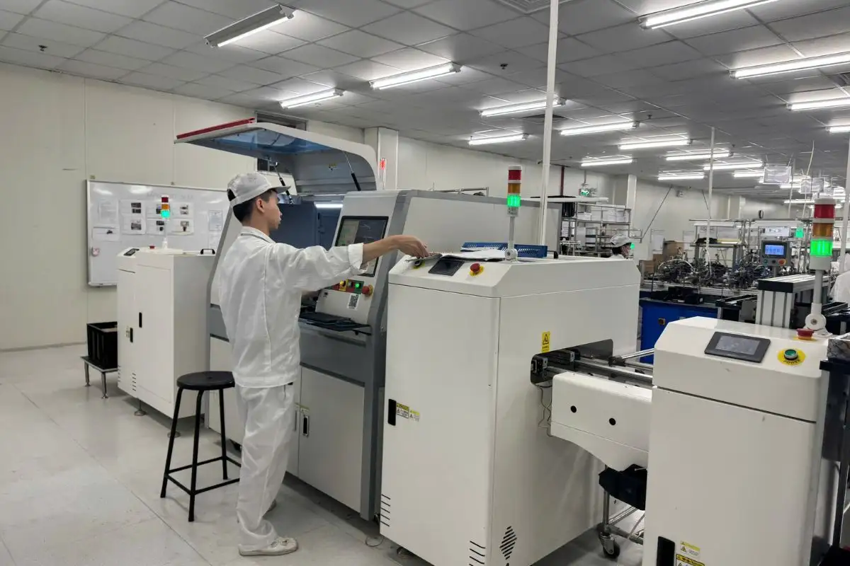
SHDC Electronics operates Vietnam’s documented GaN charger PCB assembly line at VSIP Hai Duong industrial zone. The equipment stack covers all three requirements:
| Requirement | Equipment | Status |
|---|---|---|
| Nitrogen reflow | Nitrogen reflow oven, > 1000 ppm N₂ | Operational |
| 3D X-ray inspection | CT X-ray with void measurement | Operational |
| 100% hi-pot testing | 3000VAC in-line tester | 100% in-line |
| AOI | Automated optical inspection | Post-reflow |
| Pre-compliance EMC | In-house pre-scan capability | Operational |
Workmanship standard: IPC-A-610 Class 2, with IPC-J-STD-001 soldering process compliance. Proven wattage range: 30W–140W.
For the full overview of SHDC’s electronics manufacturing capabilities, see: Electronics Manufacturing Vietnam.
Tariff Position: 0% vs 145%
GaN chargers classified under HTS 8504.40 imported from Vietnam carry a 0% MFN tariff rate. The same product from China carries 145% under Section 301. On a $9.50 factory-cost unit, that is a $13.08 per-unit landed cost advantage — before accounting for UFLPA compliance risk.
For the full cost model, see: Tariff Impact: China vs Vietnam Electronics Manufacturing.
Production Proof: Certified Products, Not Capability Claims
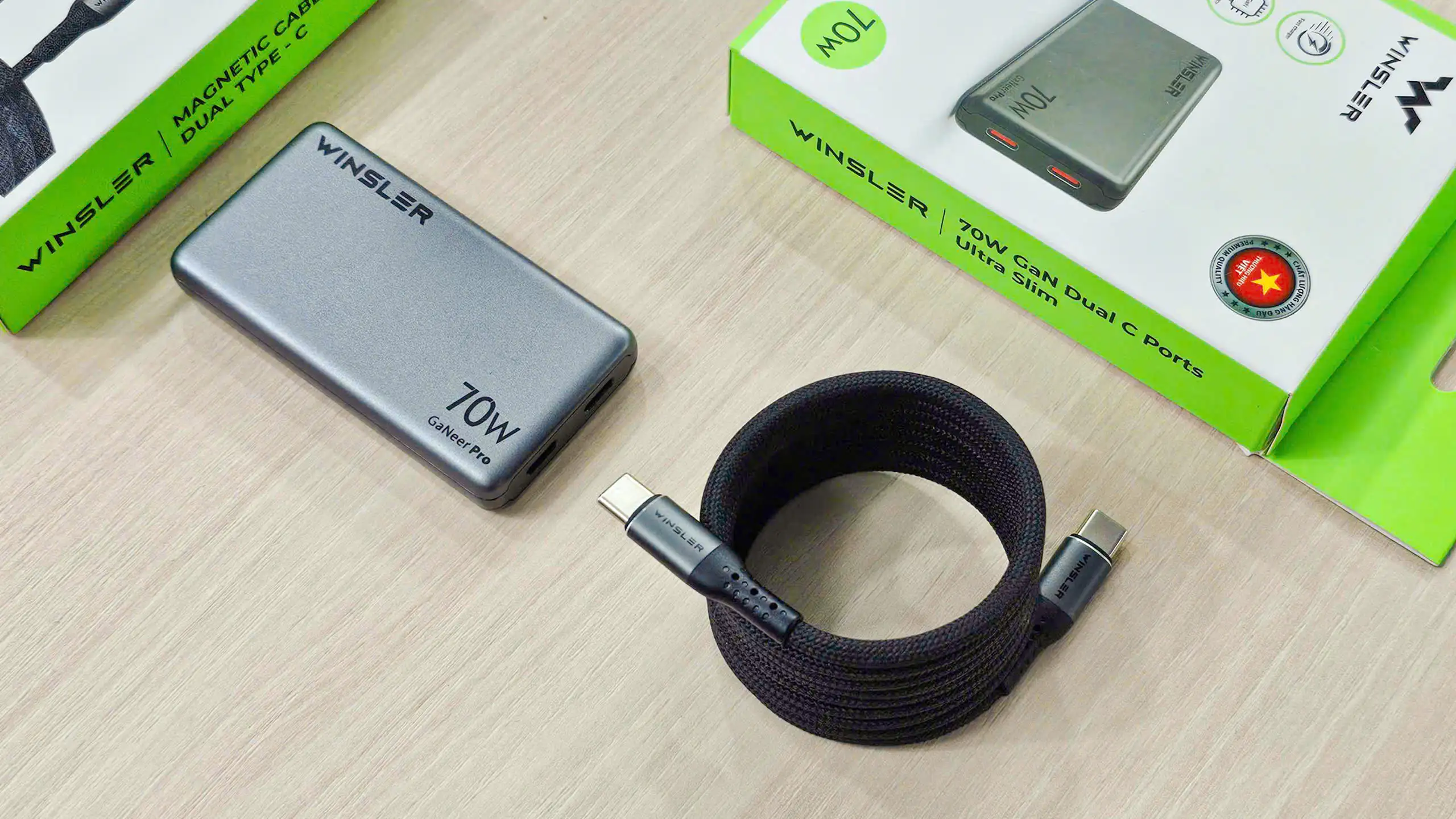
Winsler 70W Ultra Slim — SHDC’s own-brand product. ETL certified (Intertek), FCC Part 15 compliant, 12.8mm thickness, dual USB-C output. Shipped to the US market. Covered by VnExpress and Thanh Nien.
PlugBug for Twelve South — SHDC manufactured the PlugBug GaN charger line for Twelve South, a US accessories brand distributed through Apple retail channels. The program includes a 120W 4-port and 50W 2-port GaN charger, both exported to the US market. Apple supply chain qualification is among the most stringent in consumer electronics. Source: VietnamNet, February 2025.
The factory that built these products — ETL certified, FCC compliant, Apple supply chain qualified — is available for OEM programs. The learning curve has already been paid for, on SHDC’s own products.
Certification Support
SHDC supports the full US market certification stack with Tier 3 engineering involvement:
| Certification | Support Level |
|---|---|
| ETL (Intertek) | Active certificate — Winsler 70W reference |
| FCC Part 15 Class B | Active — pre-compliance scan + lab coordination |
| UL 62368-1 | Supported via accredited labs |
| USB-IF TID | Supported |
| CE Mark | Supported for EU scope |
Tier 3 support means SHDC reviews PCB layout for creepage violations and GaN loop area, runs pre-compliance EMC scans, conducts 100% in-line hi-pot before shipment, and coordinates with third-party labs — not just assembles boards and hands off a package.
For the broader context of Vietnam’s power electronics manufacturing ecosystem, see the full capability overview.
Frequently Asked Questions
What equipment is required for GaN charger PCB assembly?
The minimum equipment stack for US-market GaN charger production: nitrogen reflow oven (to control QFN thermal pad void per IPC-7093), 3D X-ray inspection (to measure and document void percentage), 100% in-line hi-pot tester at 3000VAC minimum (per UL 62368-1 isolation requirements), and AOI post-reflow. Pre-compliance EMC scanning capability is strongly recommended before lab submission.
Why does GaN charger assembly require nitrogen reflow?
GaN ICs use QFN packaging with a thermal pad on the underside. During standard air reflow, oxygen creates oxide layers that prevent complete solder wetting, resulting in voids beneath the thermal pad. Voids above 25% (IPC-7093 limit) increase thermal resistance, raise junction temperature, and shorten product lifespan. Nitrogen reflow eliminates oxygen from the reflow chamber, reducing void percentage to below 10%.
What is the IPC-7093 standard for QFN thermal pad void?
IPC-7093 — Design and Assembly Process Implementation for Bottom Termination Components — sets the maximum acceptable void percentage for QFN thermal pads at 25%. For GaN charger applications where thermal performance is critical, most manufacturers target below 15%.
Can a standard SMT factory build GaN chargers?
A standard SMT factory can assemble GaN charger PCBs — but without nitrogen reflow, 3D X-ray, and 100% hi-pot testing, the output will not reliably pass UL 62368-1 or FCC Part 15 certification. The most common outcomes are ETL/UL lab failure due to isolation issues, FCC failure due to EMI from oversized power loops, or field failures from thermal pad void exceeding IPC-7093 limits.
How long does GaN charger PCB assembly and certification take in Vietnam?
For a custom design: 20–24 weeks from DFM review to production qualification. Breakdown: DFM + layout review (2–3 weeks), PCB fabrication + prototype assembly (3–4 weeks), pre-compliance EMC scan (1 week), ETL/UL lab submission (6–10 weeks), FCC lab submission (4–6 weeks, can run parallel). For programs using an existing certified platform, timeline compresses to 12–16 weeks.
What is the difference between 2D and 3D X-ray for GaN PCB assembly?
2D X-ray produces a projected image of the solder joint — useful for detecting void presence but unable to accurately measure void percentage because it cannot resolve depth. 3D X-ray (computed tomography) reconstructs a volumetric image, enabling precise void percentage measurement with annotated output that satisfies IPC-7093 documentation requirements. For GaN charger production, 3D X-ray is the required standard.
Conclusion
The gap between a standard SMT shop and a real GaN line is not about equipment lists on a capability sheet. It is about nitrogen reflow, 3D X-ray void measurement, and 100% hi-pot testing running together — consistently, in production, on every lot.
In Vietnam, that combination exists at SHDC Hai Duong, with ETL-certified products already on the US market as proof. For US hardware teams moving GaN charger production outside China, that proof matters more than any capability claim.
