Tiếng Việt
 日本語
日本語In PCB assembly, defects are not just quality issues—they are direct cost drivers. A single soldering defect can lead to rework, scrap, delayed shipments, and in worst cases, field failures. For OEMs and engineers, understanding common PCB assembly defects, their root causes, and how they impact production yield is critical to building a stable and scalable manufacturing process. This guide breaks down defects from a real production perspective—focusing not only on what goes wrong, but how to prevent it and improve yield at scale.
Main content
ToggleWhat Are PCB Assembly Defects?
PCB assembly defects are imperfections that occur during the SMT (surface mount) or through-hole (THT) assembly process, affecting the electrical, mechanical, or thermal performance of a circuit board.
These defects can originate from:
- Process variation
- Material inconsistencies
- Design issues
- Equipment limitations
At scale, even a small defect rate can significantly reduce first-pass yield (FPY) and increase production costs.
Why PCB Assembly Defects Matter in Production
Defects are not isolated technical problems—they have a cascading impact on the entire production system.
1. Yield Loss
Every defective board reduces FPY, meaning more units require rework or replacement.
2. Increased Rework Cost
Rework is labor-intensive and introduces additional risk:
- potential damage to components
- inconsistent quality after repair
3. Production Delays
Defects disrupt workflow, causing:
- bottlenecks
- missed delivery deadlines
4. Reliability Risks
Undetected defects can lead to:
- intermittent failures
- product recalls
Key insight: Defect control is not just about quality—it is about protecting margin and ensuring production stability.
Common PCB Assembly Defects and Their Root Causes
Below are the most common defects encountered in modern PCB assembly, along with their causes and prevention strategies.
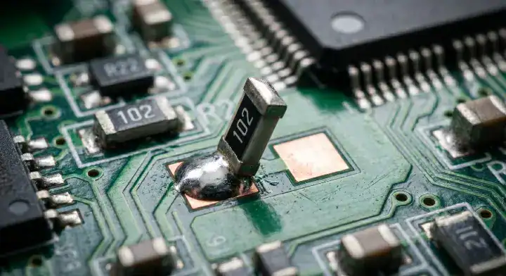
Solder Bridging
Description: Unintended solder connections between adjacent pads or pins.
Root causes:
- Excess solder paste
- Poor stencil design
- Insufficient spacing between pads
- Misalignment during placement
Impact:
- Short circuits
- Immediate functional failure
Prevention:
- Optimize stencil aperture design
- Control solder paste volume
- Improve component placement accuracy
Cold Solder Joints
Description: Weak or incomplete solder joints due to insufficient heating.
Root causes:
- Incorrect reflow temperature profile
- Poor wetting conditions
- Contaminated surfaces
Impact:
- Intermittent electrical connections
- Reduced long-term reliability
Prevention:
- Optimize thermal profiles
- Ensure proper flux activity
- Maintain clean PCB surfaces
>>>Read more: Dual In-Line Package vs Surface Mount: Key Differences in PCB Assembly
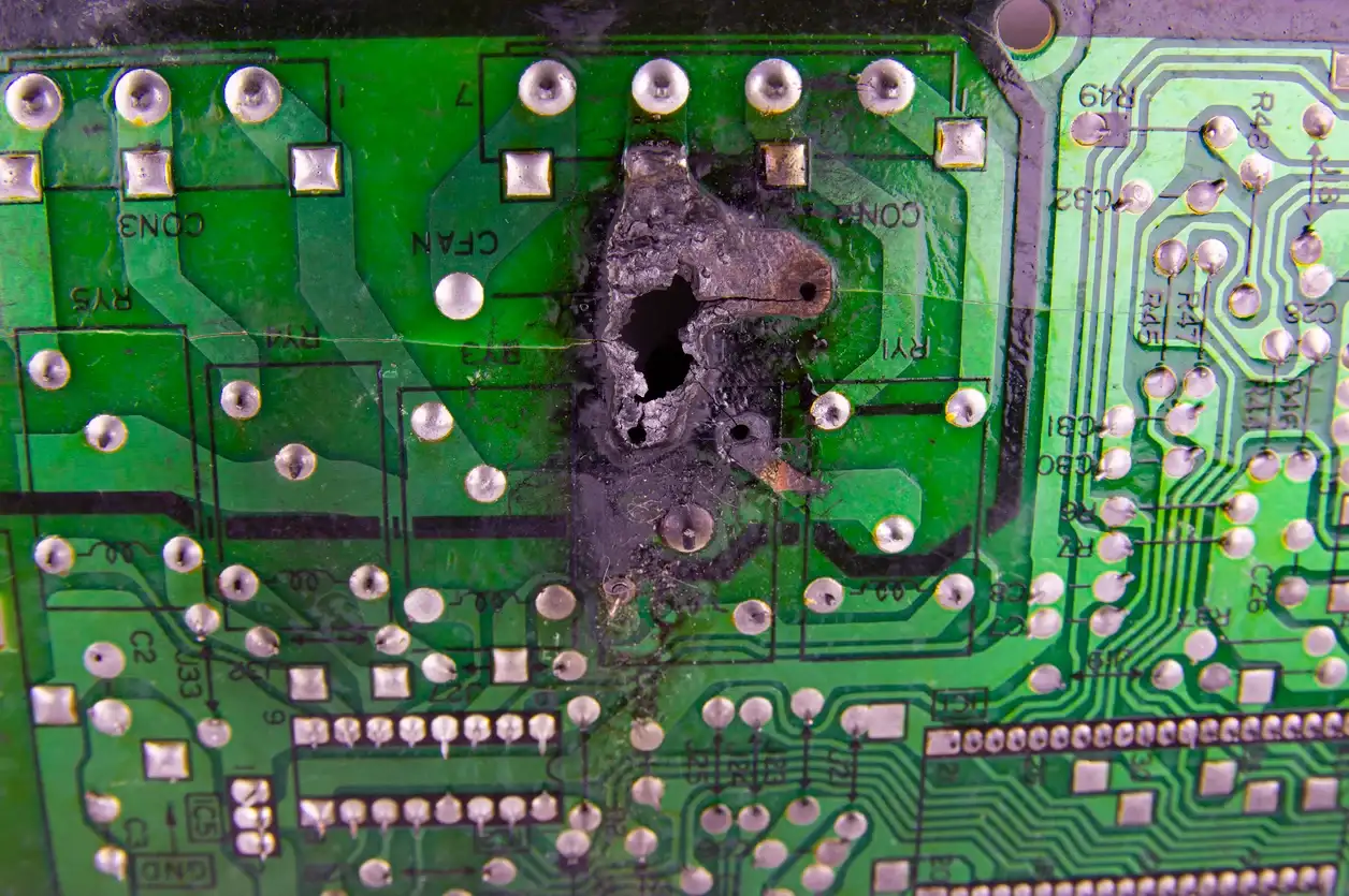
Tombstoning (SMT)
Description: One side of a component lifts during reflow, standing upright.
Root causes:
- Uneven heating across pads
- Imbalanced solder paste volume
- Component placement issues
Impact:
- Open circuits
- Assembly failure
Prevention:
- Balance pad design
- Control reflow profile
- Ensure consistent paste deposition
Voiding in Solder Joints
Description: Air pockets or voids trapped within solder joints.
Root causes:
- Outgassing during reflow
- Poor solder paste quality
- Inadequate thermal profile
Impact:
- Reduced thermal conductivity
- Lower mechanical strength
Prevention:
- Optimize reflow profile
- Use high-quality solder paste
- Improve PCB design for heat dissipation
Insufficient Solder / Poor Wetting
Description: Incomplete solder coverage on pads or leads.
Root causes:
- Oxidized surfaces
- Inadequate flux
- Incorrect temperature
Impact:
- Weak electrical connections
- Increased failure risk
Prevention:
- Ensure proper surface finish
- Maintain material quality
- Control process parameters
Component Misalignment
Description: Components placed incorrectly relative to pads.
Root causes:
- Pick-and-place calibration issues
- Warped PCBs
- Inconsistent solder paste
Impact:
- Electrical failure
- Cosmetic defects
Prevention:
- Calibrate placement machines
- Control PCB flatness
- Optimize stencil printing
Root Causes of PCB Assembly Defects
While defects appear in different forms, their root causes generally fall into four categories:
1. Process Issues
- Incorrect reflow temperature profiles
- Poor wave soldering parameters
- Inconsistent process control
Even small variations can lead to large defect rates.
2. Material Issues
- Low-quality solder paste
- Contaminated PCB surfaces
- Inconsistent component quality
Materials directly influence solderability and joint integrity.
3. Design Issues (DFM)
- Improper pad design
- Insufficient spacing
- Thermal imbalance
Poor design increases defect risk regardless of process quality.
4. Equipment and Human Factors
- Misaligned pick-and-place machines
- Poor maintenance
- Operator inconsistency
Automation reduces risk—but only when properly controlled.
>>>Read more: Wave Soldering vs Reflow Soldering: Key Differences in PCB Assembly and When to Use Each
How to Prevent PCB Assembly Defects
Defect prevention requires a system-level approach, not isolated fixes.
Design for Manufacturability (DFM)
- Optimize pad geometry
- Ensure proper spacing
- Balance thermal characteristics
Good design reduces defect risk before production begins.
Process Control
- Maintain stable reflow profiles
- Monitor wave soldering parameters
- Reduce variation across batches
Consistency is the key to high yield.
Material Quality
- Use reliable solder paste
- Ensure PCB surface cleanliness
- Maintain storage conditions
Automation and Standardization
- Use calibrated SMT equipment
- Standardize workflows
- Reduce manual variability
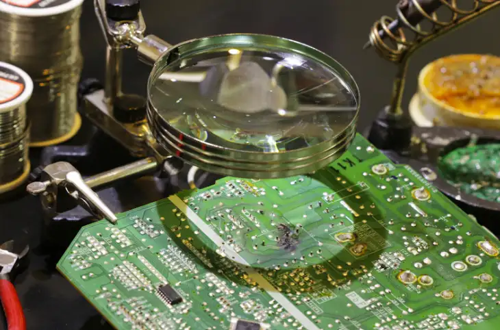
Inspection and Testing Methods to Detect Defects
Detection is critical for preventing defective products from reaching customers.
Automated Optical Inspection (AOI)
- Detects visual defects:
- misalignment
- solder bridging
- Verifies electrical connectivity
- Identifies open and short circuits
Functional Testing (FCT)
- Ensures the board operates as intended
- Detects hidden defects:
- voiding
- BGA solder issues
Insight: Inspection does not eliminate defects—but it prevents them from escaping into the field.
How PCB Assembly Defects Affect Production Yield
Production yield is one of the most critical KPIs in electronics manufacturing.
Relationship between defects and yield:
- Higher defect rate → lower first-pass yield
- Lower yield → more rework and scrap
Hidden costs of low yield:
- Increased labor
- Material waste
- Delayed delivery
Example: A 95% yield may seem acceptable—but at scale, the 5% defect rate can significantly impact profitability.
Improving Production Yield in PCB Assembly
Improving yield is not about eliminating all defects—it’s about reducing variability and controlling processes.
Key strategies:
1. Process optimization
- Fine-tune reflow profiles
- Stabilize wave soldering conditions
2. Continuous monitoring
- Use real-time data
- Track defect trends
3. Root cause analysis
- Identify recurring issues
- Implement corrective actions
4. Cross-functional alignment
- Align design, engineering, and production teams
Key insight: High yield is not achieved by chance—it is the result of a controlled and optimized system.
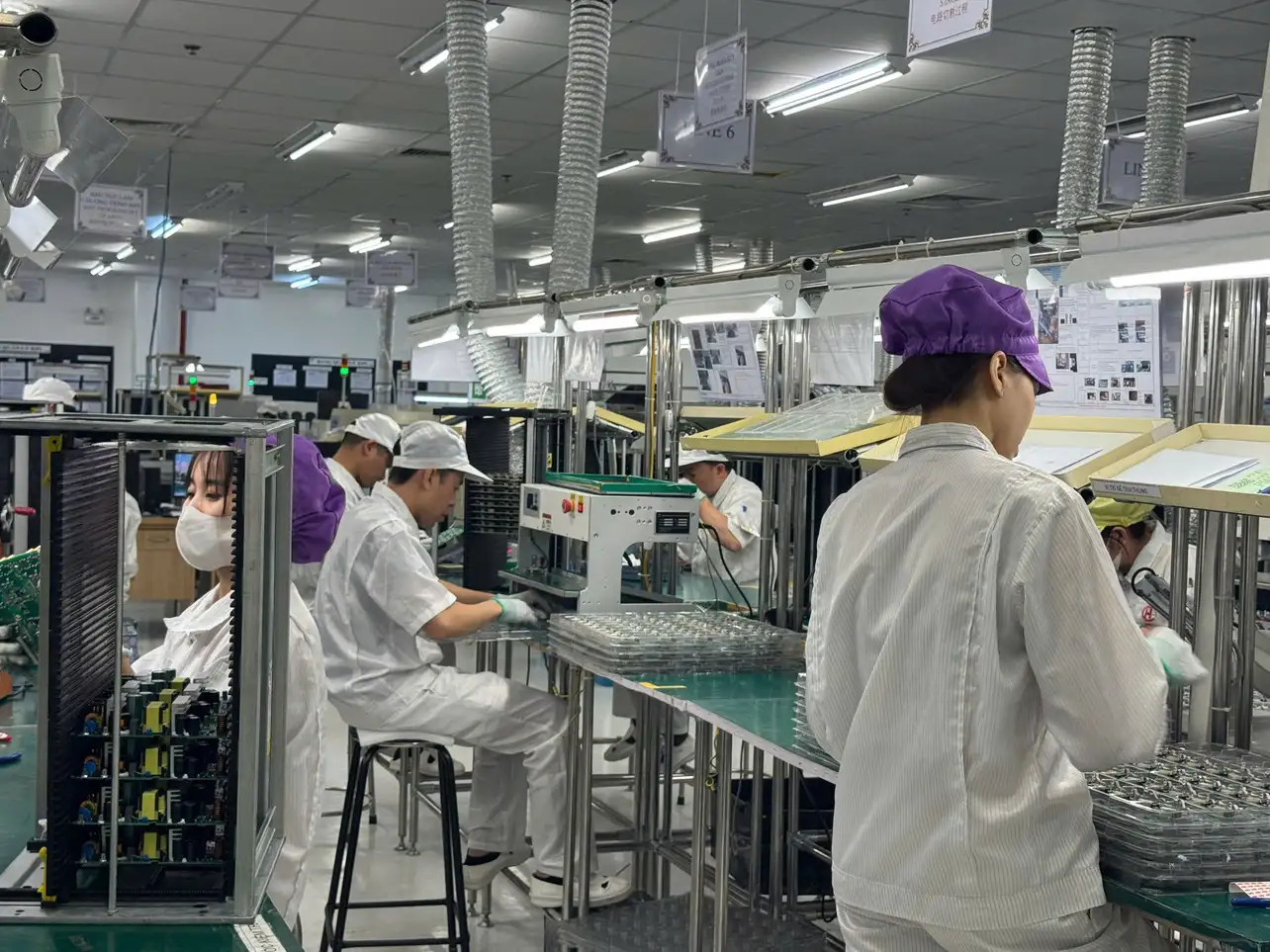
How a Reliable EMS Provider Reduces PCB Assembly Defects
For OEMs, reducing defects is not just an internal task—it depends heavily on the capabilities of the manufacturing partner.
A reliable EMS provider should:
- Implement strict process control
- Maintain equipment calibration
- Apply DFM principles early
- Integrate inspection at multiple stages
This reduces:
- defect rates
- rework
- production risk
Quality Control in High-Reliability PCB Assembly
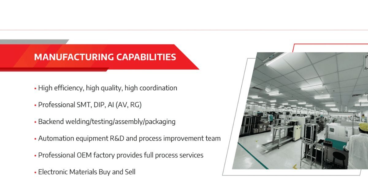
In high-reliability production environments, defect prevention is built into every stage of the process.
At SHDC, PCB assembly operations are structured around minimizing defects and maximizing yield through:
- Integrated SMT and DIP assembly processes
- Controlled soldering systems (reflow and wave)
- Multi-stage inspection (AOI, ICT, functional testing)
- Continuous process monitoring and optimization
By aligning design, materials, and manufacturing processes, production systems can achieve:
- higher first-pass yield
- lower defect rates
- improved long-term reliability
For OEMs, this translates into lower total cost and more predictable production outcomes.
FAQs
What are the most common PCB assembly defects?
Common defects include solder bridging, cold joints, tombstoning, voiding, and misalignment.
What causes PCB assembly defects?
They are typically caused by process variation, material issues, poor design, or equipment problems.
How can PCB defects be prevented?
Through proper DFM, process control, material quality, and effective inspection methods.
What is the impact of defects on production yield?
Defects reduce yield, increase rework, and raise production costs.
What testing methods detect PCB defe?
AOI, ICT, functional testing, and X-ray inspection are commonly used.
Final Thoughts
Understanding the relationship between def allows manufacturers to move from reactive troubleshooting to proactive process optimization. In modern electronics manufacturing, success is not defined by avoiding defects entirely—but by building systems that detect, co.
>>> Read more: SMT Assembly Line Equipment: Complete Guide to Machines, Line Setup & Costs