Tiếng Việt
 日本語
日本語Soldering is the most critical—and most failure-prone—stage in PCB assembly. Whether you are running high-speed SMT lines or through-hole wave soldering, defects are rarely random. They are the result of interactions between heat, materials, and process control. For OEMs and manufacturing engineers, the real challenge is not identifying defects—but understanding why they occur differently in SMT vs wave soldering, and how to systematically prevent them to protect yield and reliability. This guide takes a process-driven, mechanism-level approach to soldering defects—moving beyond surface symptoms to the underlying causes.
Why Soldering Defects Occur in PCB Assembly Processes
Soldering is fundamentally a thermo-mechanical and chemical process. A proper solder joint depends on:
- Controlled heat transfer
- Proper flux activation
- Adequate wetting between solder and metal surfaces
Defects occur when this balance is disrupted.
Key failure drivers:
- Thermal imbalance
- Poor wetting behavior
- Contamination or oxidation
- Uncontrolled solder flow
Critical insight: Soldering defects are not isolated events—they are process-driven failures. If the process is unstable, defects are inevitable.
>>>Read more: Common PCB Assembly Defects: Causes, Prevention, and How to Improve Production Yield
Key Differences Between SMT Reflow and Wave Soldering Processes
Understanding how defects form requires a clear distinction between SMT and wave soldering mechanisms.
SMT Reflow Process
- Solder paste is deposited on pads
- Components are placed
- The assembly passes through a reflow oven
- Solder melts and solidifies under a controlled temperature profile
Wave Soldering Process
- PCB passes over a of molten solder
- Solder makes direct with exposed metal
- Through-hole leads and pads are soldered simultaneously
Process Comparison
| Factor | SMT Reflow | Wave Soldering |
|---|---|---|
| Heat transfer | Gradual, controlled | Direct, high contact |
| Solder source | Paste (pre-deposited) | Liquid wave |
| Dominant physics | Thermal gradients | Fluid dynamics |
| Defect drivers | Imbalance in heating | Solder flow behavior |
Key takeaway: SMT defects are primarily driven by thermal imbalance, while wave soldering defects are largely influenced by fluid behavior and contact dynamics.
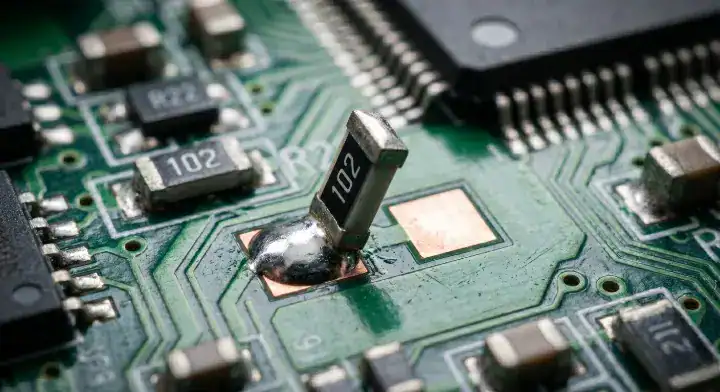
Soldering Defects in SMT: Mechanisms, Causes, and Prevention
SMT defects originate from how solder paste behaves during reflow. The key factor is how heat distribution affects melting, wetting, and solidification.
Tombstoning – Thermal Imbalance Effect
Mechanism: Uneven wetting forces on two pads cause one side of the component to lift.
Root causes:
- Uneven temperature distribution
- Imbalanced solder paste volume
- Asymmetric pad design
Impact:
- Open circuits
- Assembly failure
Prevention:
- Optimize pad symmetry
- Balance solder paste deposition
- Fine-tune reflow profile to ensure uniform heating
Solder Bridging – Paste Volume and Placement Interaction
Mechanism: Excess molten solder flows between adjacent pads, creating unintended connections.
Root causes:
- Excess solder paste
- Poor stencil design
- Misalignment during placement
Impact:
- Short circuits
- Immediate functional failure
Prevention:
- Optimize stencil aperture design
- Control paste volume precisely
- Improve placement accuracy
Voiding – Outgassing and Reflow Dynamics
Mechanism: Gas trapped within molten solder creates voids as it solidifies.
Root causes:
- Volatile materials in solder paste
- Rapid heating during reflow
- Poor thermal profile design
Impact:
- Reduced thermal conductivity
- Lower mechanical strength
Prevention:
- Use high-quality solder paste
- Optimize ramp-up temperature
- Improve PCB design for heat dissipation
Cold Solder Joints – Incomplete Reflow
Mechanism: Solder does not fully melt or properly wet the surfaces.
Root causes:
- Insufficient peak temperature
- Inadequate soak time
- Oxidized pads or leads
Impact:
- Intermittent electrical failures
- Long-term reliability issues
Prevention:
- Validate reflow profiles
- Maintain clean surfaces
- Ensure proper flux activation
>>>Read more: Dual In-Line Package vs Surface Mount: Key Differences in PCB Assembly
Soldering Defects in Wave Soldering: Flow Behavior and Process Risks
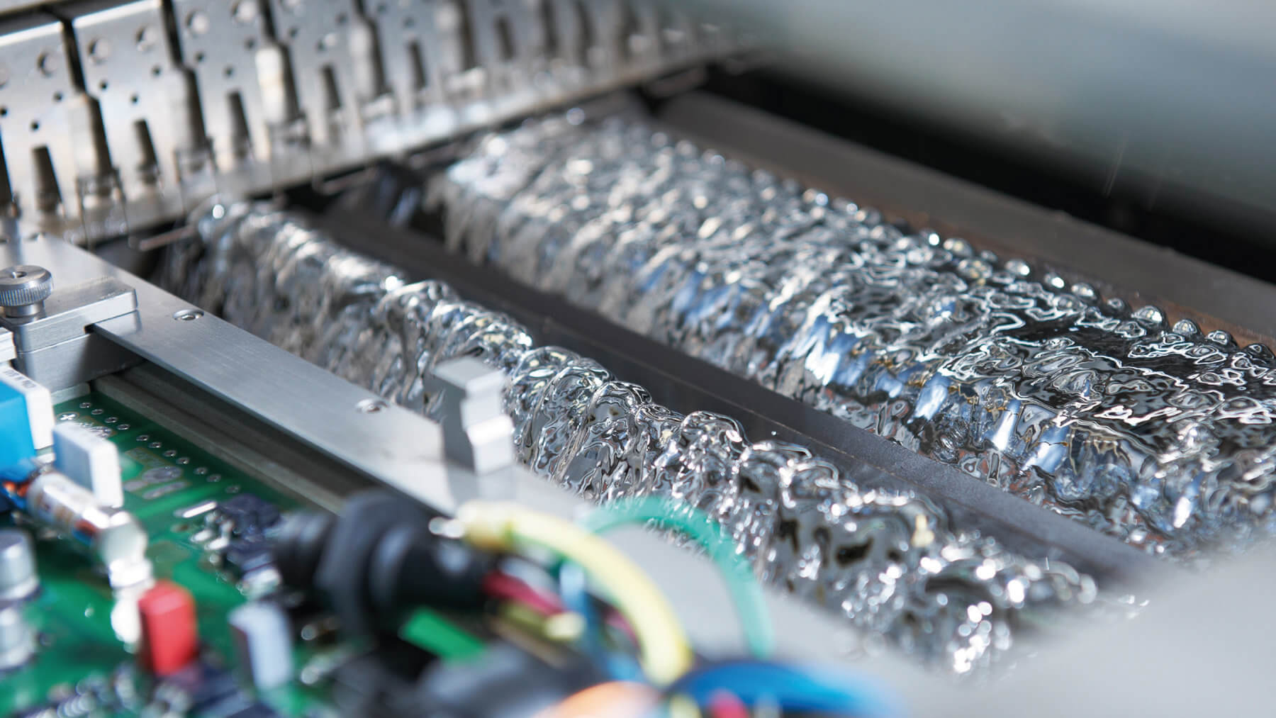
Wave soldering defects are governed by fluid dynamics and thermal shock, rather than controlled thermal profiles.
Solder Bridging – Excessive Wave Contact
Mechanism: Molten solder forms unintended connections as it flows between adjacent leads.
Root causes:
- Slow conveyor speed
- High wave height
- Poor PCB orientation
Impact:
- Short circuits
- Functional failure
Prevention:
- Optimize conveyor speed
- Adjust wave height and turbulence
- Improve PCB layout spacing
Icicles and Solder Spikes – Withdrawal Dynamics
Mechanism: Solder is pulled into spikes as the board exits the wave.
Root causes:
- Improper withdrawal angle
- Excess solder
- Poor surface tension control
Impact:
- Mechanical defects
- Risk of shorts
Prevention:
- Optimize board exit angle
- Control solder viscosity
- Adjust cooling conditions
Non-Wetting – Surface and Flux Issues
Mechanism: Solder fails to adhere to the metal surface.
Root causes:
- Oxidation
- Insufficient flux
- Contaminated surfaces
Impact:
- Open circuits
- Weak joints
Prevention:
- Ensure proper flux application
- Maintain clean PCB surfaces
- Control preheat conditions
Blow Holes – Gas Expansion in Through-Hole
Mechanism: Moisture or trapped gases expand during soldering.
Root causes:
- Moisture in PCB
- Rapid temperature increase
Impact:
- Structural defects in solder joints
- Reduced reliability
Prevention:
- Pre-bake PCBs
- Control thermal ramp rate
>>>Read more: Wave Soldering vs Reflow Soldering: Key Differences in PCB Assembly and When to Use Each
Root Cause Analysis: Why the Same Defect Occurs Differently in SMT vs Wave
One of the most overlooked insights in PCB assembly is that the same defect name does not mean the same root cause.
- In SMT:
- Caused by excess solder paste
- Driven by stencil design and placement accuracy
- In Wave Soldering:
- Caused by uncontrolled solder flow
- Driven by wave dynamics and PCB orientation
Key insight: Effective defect prevention requires understanding the process-specific mechanism, not just the visible symptom.
Process Optimization Strategies to Prevent Soldering Defects
Defect reduction starts with process control—not inspection.
SMT Process Optimization
- Optimize reflow temperature profiles
- Control solder paste deposition
- Ensure precise component placement
- Reduce thermal variation across the board
Wave Soldering Optimization
- Adjust wave height and turbulence
- Control conveyor speed
- Optimize flux application
- Ensure proper preheating
Key takeaway: SMT requires thermal precision, while wave soldering requires flow control stability.
Role of Materials in Soldering Defect Formation
Materials are often the hidden variable in defect formation.
Critical material factors:
- Solder paste composition
- Flux chemistry
- PCB surface finish (OSP, ENIG, HASL)
Even with a stable process, poor material quality can introduce:
- inconsistent wetting
- voiding
- oxidation-related defects
Inspection and Detection of Soldering Defects
Detection systems play a critical role in quality assurance—but they are not a substitute for process control.
Common methods:
- AOI: visual defect detection
- X-ray: internal joint analysis
- ICT: electrical validation
- Functional testing: real-world performance
Important: Inspection catches defects—but only process control prevents them.
Impact of Soldering Defects on Yield and Reliability
Soldering defects are one of the primary causes of yield loss in PCB assembly.
Production impact:
- Increased rework
- Higher scrap rates
- Reduced throughput
Business impact:
- Increased cost
- Delayed delivery
- Reduced customer satisfaction
Key insight: Soldering defects are not just technical issues—they are profit and risk factors.
>>>Read more: PCB Board Fabrication vs PCB Assembly: What OEMs Need to Know Before Production
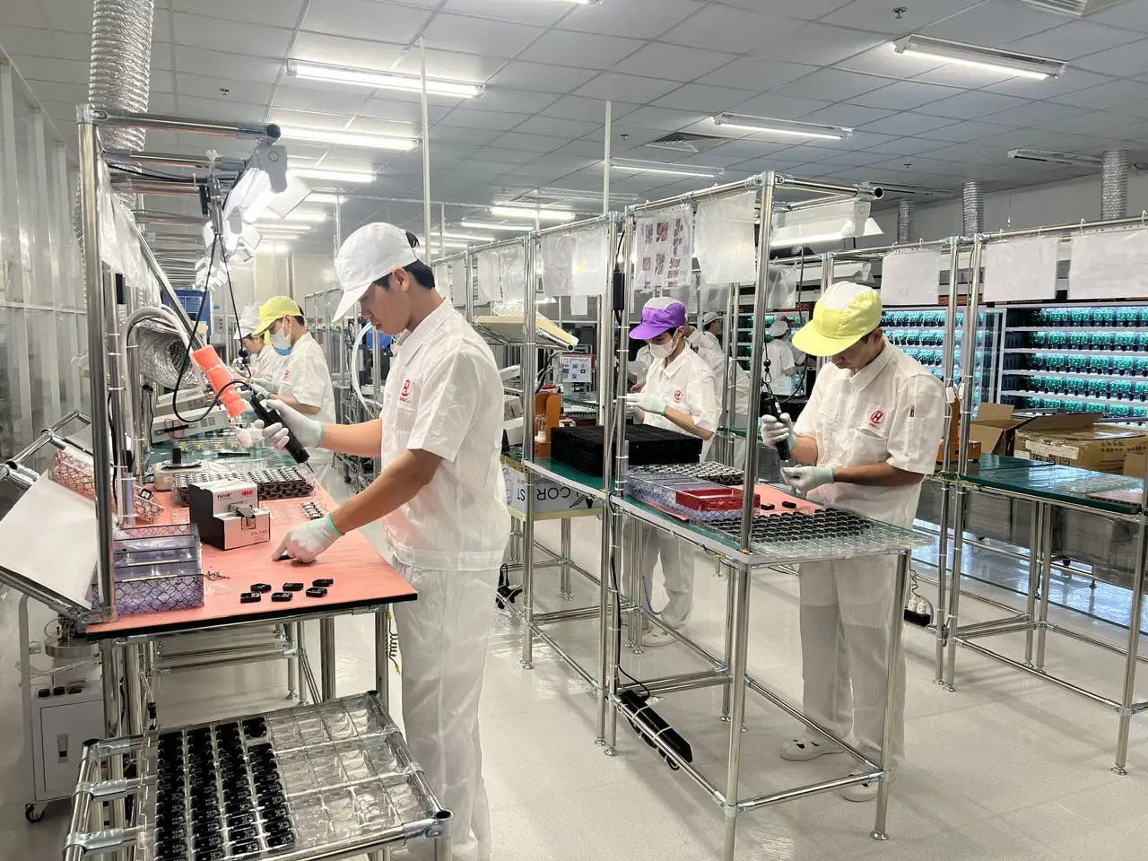
How Advanced EMS Providers Control Soldering Quality
For OEMs, controlling soldering defects depends heavily on manufacturing capability.
A qualified EMS provider will:
- Maintain strict process control
- Monitor thermal profiles and wave parameters
- Implement real-time quality tracking
- Integrate inspection into the production flow
Process Control in High-Reliability PCB Assembly

At SHDC, soldering quality is managed through a combination of process control, material selection, and inspection systems.
This includes:
- Controlled SMT reflow profiles to ensure consistent solder joint formation
- Optimized wave soldering parameters for stable through-hole assembly
- Material verification to reduce variability
- Multi-stage inspection to detect and isolate defects early
By focusing on process stability rather than reactive correction, manufacturers can:
- improve first-pass yield
- reduce defect rates
- ensure long-term product reliability
>>>Read more: SHDC Contract Electronics Manufacturing Services for OEM Companies in Vietnam
FAQs
What are the most common soldering defects in SMT?
Tombstoning, solder bridging, voiding, and cold joints are among the most common.
What causes defects in wave soldering?
Defects are typically caused by solder flow behavior, improper fluxing, and thermal shock.
Why does the same defect occur differently in SMT and wave soldering?
Because the underlying mechanisms—thermal vs fluid dynamics—are different.
How can soldering defects be prevented?
Through process optimization, proper material selection, and design for manufacturability.
How do soldering defects affect PCB reliability?
They can lead to intermittent failures, reduced lifespan, and increased risk of product failure.
Final Thoughts
Soldering defects are not random—they are predictable outcomes of process conditions. By understanding the mechanisms behind defect formation in SMT and wave soldering, manufacturers can shift from reactive troubleshooting to proactive process control. In modern PCB assembly, success is not about eliminating defects entirely—it’s about building systems that minimize variability, control risk, and consistently deliver high yield at scale.
>>>Read more: Global Electronics Manufacturing Services: Comparing Asia, North America, and Emerging Markets for OEM Companies