Tiếng Việt
 日本語
日本語The circuit board fabrication process is the engineering foundation behind every reliable electronic product. From multilayer industrial control systems to high-density consumer electronics, fabrication quality directly determines electrical performance, durability, and long-term reliability. Understanding how circuit board fabrication works — including materials, process control, and industry standards — is essential for OEMs, engineers, and sourcing professionals operating in today’s global electronics supply chain.
What Is Circuit Board Fabrication?
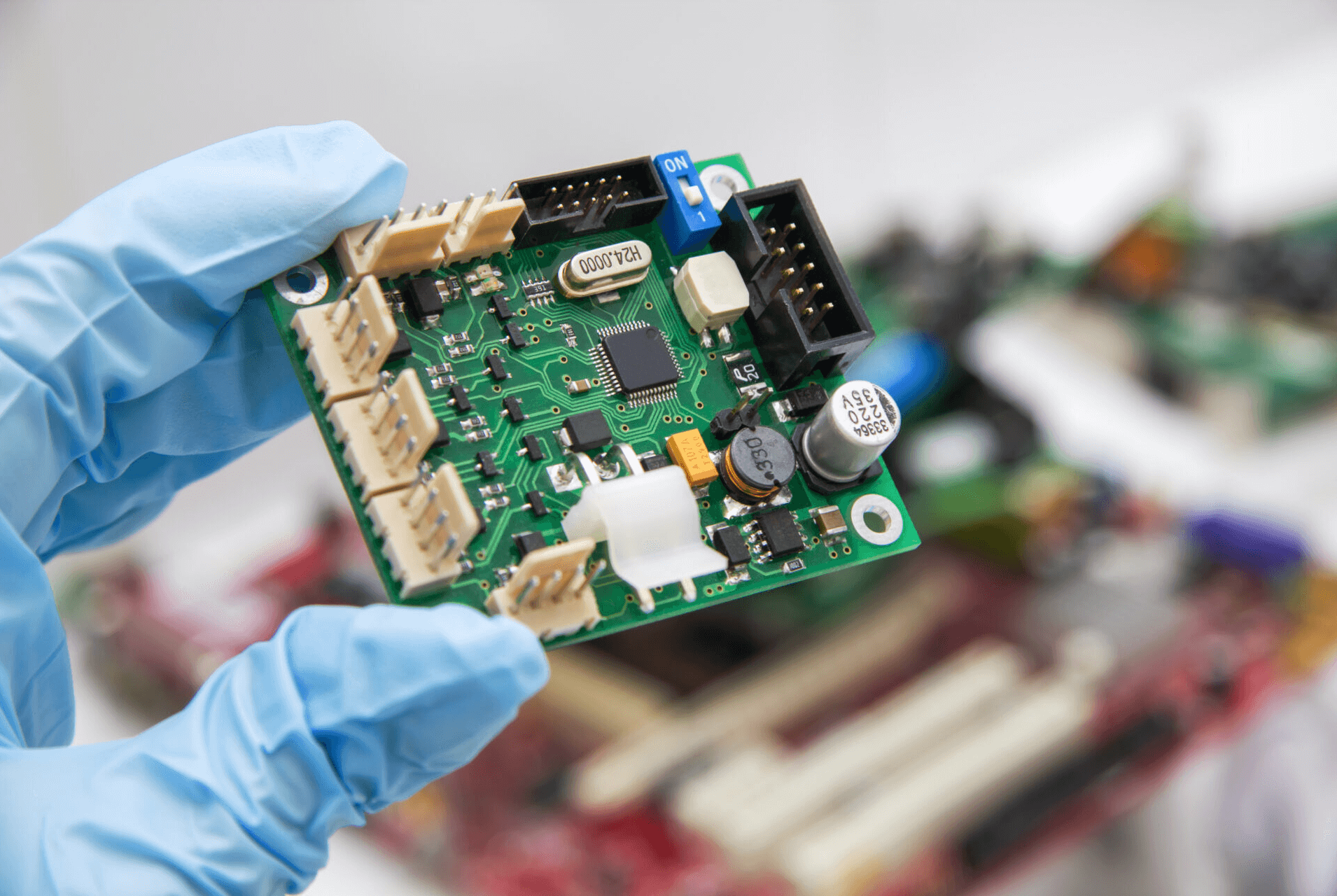
Circuit board fabrication refers specifically to the manufacturing of the bare printed circuit board (PCB) before components are mounted. It includes:
-
Layer imaging
-
Copper etching
-
Lamination
-
Drilling and via formation
-
Plating
-
Surface finishing
-
Electrical testing
It does not include component placement or soldering — those steps belong to PCB assembly (PCBA).
In professional electronics manufacturing, fabrication precision determines:
-
Signal integrity
-
Thermal stability
-
Mechanical durability
-
Long-term field reliability
Even minor fabrication defects can lead to latent failures, making strict process control critical.
>>>Read more: PCB Manufacturing Process: Step-by-Step Guide
Overview of the Circuit Board Fabrication Process
While fabrication complexity varies depending on board type (2-layer, 4-layer, HDI, flex), the process generally follows these stages:
-
Design file review and DFM analysis
-
Laminate preparation
-
Inner layer imaging and etching
-
Layer stacking and lamination
-
Drilling (mechanical or laser)
-
Copper plating
-
Outer layer processing
-
Solder mask and surface finish
-
Final electrical testing
Each stage must comply with recognized industry standards to ensure consistency and performance.
Step-by-Step Circuit Board Fabrication Process
1. Design File Review and DFM Analysis
Fabrication begins with a review of Gerber files and stack-up specifications. Engineering teams verify:
-
Trace width and spacing
-
Annular ring size
-
Via aspect ratios
-
Controlled impedance requirements
-
Layer alignment tolerances
Compliance with IPC-2221 design standards is typically evaluated at this stage. Early DFM review reduces scrap rates and improves yield in production.
2. Material Selection and Laminate Preparation
Material selection significantly impacts performance. Common materials include:
FR-4
Standard glass-reinforced epoxy laminate used in most applications.
High-Tg Laminates
Used for higher thermal resistance in industrial or automotive environments.
Rogers Materials
Selected for RF and high-frequency designs due to stable dielectric properties.
Polyimide
Applied in flexible PCB fabrication.
Key performance factors include:
-
Tg (glass transition temperature)
-
Dielectric constant (Dk)
-
Coefficient of thermal expansion (CTE)
-
Copper thickness (1 oz, 2 oz, etc.)
Improper material choice can compromise signal integrity and reliability.
3. Inner Layer Imaging and Etching
For multilayer boards, inner copper layers are processed first:
-
Photoresist application
-
UV exposure
-
Developing
-
Chemical etching
Precision in this stage ensures consistent line width and spacing. Over-etching can weaken traces; under-etching can cause shorts.
4. Layer Alignment and Lamination
Multiple layers are stacked with prepreg insulation and laminated under controlled temperature and pressure.
Registration accuracy is critical — misalignment can cause via breakout and connectivity failure.
Multilayer fabrication complexity increases exponentially with layer count (6-layer, 8-layer, 12-layer boards and beyond).
5. Drilling and Via Formation
After lamination, drilling creates:
-
Through-hole vias
-
Blind vias
-
Buried vias
-
Mounting holes
Mechanical drilling is common for standard PCBs. Laser drilling is used for HDI microvias.
Aspect ratio control ensures reliable copper plating later.
6. Copper Plating and Via Metallization
Drilled holes are made conductive through:
-
Electroless copper deposition
-
Electrolytic copper plating
IPC-6012 specifies minimum plating thickness for structural reliability. Poor metallization can cause intermittent failures in field use.
7. Outer Layer Imaging and Final Etching
Outer copper layers are patterned similarly to inner layers. This stage defines final signal routing and pad geometry.
Copper balancing is important to prevent warping.
8. Solder Mask Application
Liquid Photoimageable (LPI) solder mask is applied to:
-
Protect copper traces
-
Prevent solder bridging
-
Improve environmental durability
Proper thickness and alignment are critical for assembly reliability.
9. Surface Finishes
Surface finish protects exposed copper and ensures solderability.
Common finishes include:
– ENIG (Electroless Nickel Immersion Gold)
Excellent for fine-pitch and high-reliability applications.
– HASL (Hot Air Solder Leveling)
Cost-effective and widely used.
– OSP (Organic Solderability Preservative)
Flat surface, lower cost, shorter shelf life.
Surface finish choice impacts cost, shelf life, and long-term reliability.
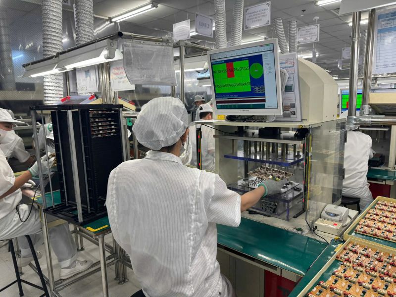
10. Electrical Testing and Inspection
Before shipment, fabricated boards undergo:
-
AOI (Automated Optical Inspection)
-
Flying probe testing
-
Electrical continuity testing
-
X-ray inspection for complex structures
Electrical testing ensures no opens or shorts exist before assembly.
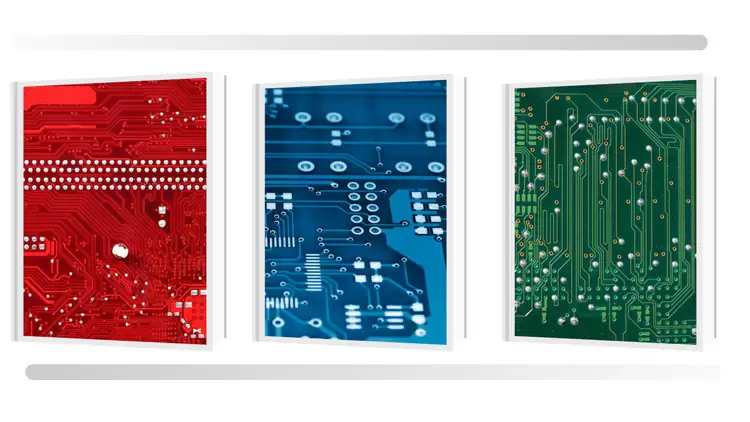
Materials Used in Circuit Board Fabrication

Material engineering is one of the most critical aspects of fabrication.
Key materials include:
-
Copper foil (rolled or electrodeposited)
-
Glass fiber-reinforced laminates
-
Prepreg bonding sheets
-
Surface finish chemicals
-
Solder mask polymers
Material quality affects:
-
High-frequency performance
-
Thermal cycling resistance
-
Long-term mechanical stability
For US OEMs, material traceability and compliance documentation are essential.
>>>Read more: China Alternative Electronics Manufacturing: Why Vietnam Is the Top Choice in 2026
Industry Standards in Circuit Board Fabrication
Professional fabrication must comply with internationally recognized standards:
IPC-2221
Generic design standard for printed boards.
IPC-6012
Qualification and performance specification for rigid PCBs.
IPC-A-600
Acceptability criteria for printed boards.
Additional compliance requirements include:
-
ISO 9001 certification
-
UL certification
-
RoHS environmental compliance
Adherence to these standards ensures consistency across global supply chains.
How to Evaluate a Circuit Board Fabrication Partner
When selecting a fabrication supplier, evaluate:
-
Multilayer capability
-
HDI capability
-
Minimum trace/space tolerance
-
Controlled impedance experience
-
Testing capability
-
Quality certifications
-
Production traceability systems
Manufacturers integrating fabrication with advanced assembly and quality control systems often provide stronger end-to-end reliability.
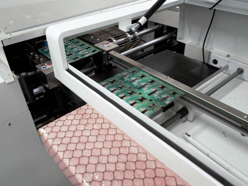
For example, SHDC, located in VSIP Hai Duong Industrial Park, operates integrated SMT production lines supported by ERP, MES, PLM, and QMS systems. With ISO-certified management, 3D AOI inspection, ICT and FCT testing capability, and the ability to handle PCB sizes from 50×50 mm to 460×550 mm — including fine-pitch components down to 0201 — SHDC demonstrates how disciplined process control and engineering oversight support global electronics manufacturing requirements.
While fabrication precision forms the structural foundation of a PCB, integrated quality systems across fabrication and assembly stages further reduce risk for OEM clients.
Common Fabrication Defects and Prevention
Understanding common fabrication defects improves supplier evaluation:
-
Delamination due to improper lamination control
-
Via voids from inadequate plating
-
Misregistration between layers
-
Over-etching or under-etching
-
Solder mask misalignment
Robust quality systems and in-process inspection significantly reduce these risks.
Frequently Asked Questions
What is the difference between PCB fabrication and PCB manufacturing?
Fabrication refers to creating the bare board. PCB manufacturing often includes both fabrication and assembly.
How long does circuit board fabrication take?
Prototypes may require 5–7 business days; production runs typically range from 2–4 weeks depending on complexity.
What materials are best for high-frequency applications?
Rogers and other low-loss laminates provide stable dielectric properties for RF designs.
Why are IPC standards important?
They define performance and acceptability requirements that ensure reliability and consistency.
Final Thoughts
Circuit board fabrication is a precision-driven engineering process that directly influences the reliability and electrical performance of finished electronic products. From material selection and multilayer lamination to via metallization and surface finishing, each step must comply with strict industry standards and quality control protocols.
For OEMs and sourcing professionals in the US market, partnering with manufacturers that combine fabrication expertise, certified quality systems, and integrated production management reduces long-term risk and improves scalability in global electronics manufacturing.