Tiếng Việt
 日本語
日本語
A PCBA can be well designed and assembled, but if it cannot be tested efficiently, production quality becomes harder to control. Design for Testability helps electronics OEMs make products easier to inspect, test, diagnose, and validate before pilot run or mass production. For OEMs working with an EMS partner, DFT reduces test delays, improves fault detection, supports better troubleshooting, and helps every production unit meet defined quality requirements.
What Is Design for Testability?

Design for Testability, commonly called DFT, is the practice of designing a PCB or electronic product so it can be tested efficiently, consistently, and reliably during production.
In PCBA manufacturing, DFT focuses on making electrical faults, assembly issues, programming problems, and functional failures easier to detect before the product leaves the factory. This includes test point placement, ICT access, FCT planning, AOI visibility, firmware programming access, fixture design, and test documentation.
The goal of DFT is not only to confirm that a product works. The real goal is to make every unit testable at production scale. A design that is difficult to test may still pass a prototype build, but it can create serious problems when hundreds, thousands, or millions of units need to be inspected and verified.
Why Design for Testability Matters in Electronics Manufacturing
Testing is one of the most important controls in electronics production. Without good testability, manufacturers may struggle to find defects, isolate root causes, or confirm product quality before shipment.
Poor testability can lead to:
- Low test coverage
- Longer test cycle time
- More manual inspection work
- Difficult troubleshooting
- Missed soldering or component defects
- Inconsistent pass/fail decisions
- Higher rework cost
- Pilot production delays
- Lower confidence in outgoing quality
For OEMs, these issues can increase total production cost and delay product launch. For EMS partners, unclear test requirements make it harder to prepare fixtures, define inspection flow, and control quality records.
That is why DFT should be considered early, together with DFM for electronics manufacturing, BOM review, PCB layout review, and production readiness planning.
Design for Testability vs Design for Manufacturing
Design for Testability and Design for Manufacturing are closely related, but they are not the same.
| Concept | Full Name | Main Focus | PCBA Example |
|---|---|---|---|
| DFM | Design for Manufacturing | Can the board be manufactured efficiently? | PCB spacing, pad design, panelization |
| DFA | Design for Assembly | Can the product be assembled easily? | Connector access, enclosure fit, cable routing |
| DFT | Design for Testability | Can the board be tested reliably? | Test points, ICT access, FCT fixture |
| DFX | Design for Excellence | Broader optimization | Cost, quality, reliability, serviceability |
DFM helps make the product easier to build. DFT helps make the product easier to verify.
In real PCBA production, both are necessary. For example, a board may have good component placement for the SMT assembly process, but if the test points are blocked by tall components, ICT testing may still be difficult. Likewise, a product may pass functional testing, but if the process cannot detect component-level defects, quality risk remains.
Why DFT Is Important for Electronics OEMs
Better Fault Detection During Production
A strong DFT strategy helps detect problems such as opens, shorts, wrong components, reversed polarity, solder defects, missing parts, programming errors, and functional failures.
Different test methods detect different issues. Automated optical inspection can identify visible assembly defects. In-circuit testing can check electrical connections and component-level faults. Functional testing verifies whether the PCBA performs as expected in operating conditions.
When DFT is done properly, these methods work together to improve defect detection and reduce risk before shipment.
Faster Testing and Troubleshooting
Testability affects test speed. If test points are accessible, fixtures are planned early, and pass/fail criteria are clear, production testing becomes faster and more repeatable.
Good DFT also helps engineers troubleshoot failed units. Instead of spending time manually tracing signals or guessing root causes, the production team can use defined access points, test procedures, and diagnostic steps.
More Reliable Pilot Runs
Pilot production is not only about checking whether the product can be assembled. It is also the stage where test coverage, fixture design, test time, failure handling, firmware programming, and quality records should be validated.
A product that is not test-ready can delay pilot production. OEMs may need to revise PCB layouts, add test points, redesign fixtures, or rewrite test procedures. These changes are more expensive when discovered late.
A structured Production Readiness Checklist should include DFT review before moving to mass production.
Stronger Quality Control Before Shipment
Testing is directly connected to outgoing quality. If the test process is unclear or incomplete, failed units may pass through production unnoticed.
DFT supports stronger quality control by making inspection and testing more consistent. It also supports better traceability, test data recording, retest rules, and failure analysis.
How DFT Applies to PCBA Manufacturing

Test Point Design
Test points are one of the most important parts of Design for Testability. They allow probes, fixtures, and engineers to access electrical nets during ICT, debugging, programming, or functional validation.
OEMs should review:
- Are test points included for critical nets?
- Are power and ground accessible?
- Are test pads large enough for probes?
- Is there enough spacing between test points?
- Are test points away from tall components?
- Are test points placed on one side where possible?
- Are high-speed or sensitive signals handled carefully?
- Are test points clearly documented in the test point map?
A board with poor test point access may require manual workarounds, which can increase test time and reduce consistency.
ICT Access
ICT, or in-circuit testing, requires physical access to electrical nodes on the board. It is commonly used to detect opens, shorts, resistance issues, component placement errors, and some soldering defects.
For ICT readiness, OEMs should consider:
- Probe access
- Test pad size
- Test point spacing
- Fixture compatibility
- Bottom-side access
- Power and ground coverage
- Critical net coverage
- Components that cannot be easily tested through ICT
ICT is not always required for every product, but for complex PCBA or higher-volume production, it can be a valuable quality control method. The key is to plan ICT access during PCB design, not after the layout is frozen.
Functional Testing Access
Functional circuit testing, or FCT, verifies whether the product performs its intended functions. It usually checks power behavior, signal output, communication, firmware, sensors, buttons, LEDs, motors, relays, or connected loads.
A good FCT plan should define:
- Power input conditions
- Output signals
- Communication protocols
- Load simulation
- Button or sensor simulation
- Required firmware version
- Pass/fail criteria
- Test cycle time
- Data recording requirements
- Failure handling process
FCT is often closer to real product usage than ICT, but it may not identify every component-level fault. That is why the right test strategy may combine AOI, ICT, FCT, visual inspection, and final quality control.
AOI and Visual Inspection Access
AOI works best when components, solder joints, markings, and polarity indicators are visible. If tall components block inspection areas, or if markings are unclear, AOI effectiveness may be reduced.
OEMs should check:
- Are component markings visible?
- Are polarity marks clear?
- Are solder joints accessible for optical inspection?
- Are similar-looking components easy to distinguish?
- Are tall components blocking inspection?
- Are inspection standards clearly defined?
A PCB layout that supports AOI can reduce manual inspection workload and improve consistency.
Firmware Programming and Debug Access
Many modern PCBAs require firmware programming before functional testing. If programming access is not planned, production can slow down significantly.
OEMs should define:
- Programming connector or pads
- SWD, JTAG, UART, or other debug access
- Firmware version control
- Programming sequence
- Security lock or read-protection requirements
- Serial number or label tracking
- Programming verification method
Firmware and programming instructions should be included in the manufacturing documentation before production starts.
Key Elements of a Good DFT Strategy
Test Coverage
Test coverage defines what the production test process can detect. OEMs should identify the most important functions, circuits, and risks before selecting a test method.
Typical test coverage areas include:
- Power rails
- Ground continuity
- Critical ICs
- Communication interfaces
- Sensors
- LEDs and indicators
- Connectors
- Safety-related circuits
- Firmware programming
- Final product functions
No single test method covers everything. A practical DFT strategy combines methods based on product complexity, risk level, volume, and quality requirements.
>>>Read more: Production Readiness Checklist: 20 Essential Steps Before Mass Production
Test Method Selection
| Test Method | Main Purpose | Best Used For |
|---|---|---|
| AOI | Visual inspection | Placement, polarity, solder defects |
| SPI | Solder paste inspection | Paste volume and printing quality |
| ICT | Circuit-level testing | Opens, shorts, component-level faults |
| FCT | Functional testing | Product behavior and performance |
| Aging Test | Stability screening | Products requiring burn-in or reliability checks |
| High Voltage Test | Safety or insulation check | Power-related products where applicable |
The selected test method should match the product risk. For example, a simple consumer board may need AOI and FCT, while a more complex industrial or power-related PCBA may require additional ICT, aging, or high-voltage testing.
Fixture Planning
Test fixtures should be planned early because they affect PCB layout, test point placement, mechanical access, test speed, and operator workflow.
Fixture planning may include:
- Bed-of-nails fixture
- Functional test fixture
- Cable harness
- Power supply
- Load simulator
- Mechanical positioning
- Safety protection
- Operator interface
- Test software
- Data logging
If the fixture is considered too late, the PCB may not provide enough access for efficient testing.
Test Time and Production Volume
A test method can be technically correct but still impractical if it takes too long for the target production volume. OEMs should consider test cycle time early.
Important questions include:
- How long does each unit take to test?
- Can the test be automated?
- How many operators are needed?
- How are failed units handled?
- Is retesting required?
- Is test data recorded automatically?
- Does the test process match the production schedule?
For mass production, test time directly affects throughput, labor, and delivery planning.
Design for Testability Checklist for Electronics OEMs

PCB Test Point Checklist
Before releasing PCB files, OEMs should check:
- Are all critical nets accessible?
- Are power rails accessible?
- Are ground points available?
- Are test pads large enough?
- Is spacing suitable for probes?
- Are test points placed away from tall components?
- Are test points protected from accidental shorting?
- Are test points documented clearly?
- Are programming pads included if needed?
- Are high-speed or sensitive signals treated carefully?
ICT Checklist
If ICT is required, review:
- Is expected ICT coverage defined?
- Are test points located on the correct side?
- Are probe locations compatible with fixture design?
- Are components too close to test pads?
- Are no-connect pins documented?
- Are special nets documented?
- Are power and ground nets accessible?
- Are programming or calibration steps separate from ICT?
ICT planning should be discussed with the EMS partner before the final PCB layout is approved.
FCT Checklist
For functional testing, confirm:
- Is the test procedure written?
- Are pass/fail limits clear?
- Are power input conditions defined?
- Are communication protocols documented?
- Are sensors, buttons, LEDs, motors, or loads simulated?
- Is firmware required before FCT?
- Is test data recorded?
- Is retest procedure defined?
- Are failure categories documented?
A vague FCT procedure can create inconsistent results between prototype, pilot, and mass production.
AOI and Visual Inspection Checklist
For inspection readiness, check:
- Are component markings visible?
- Are polarity indicators clear?
- Are solder joints visible?
- Are similar components easy to distinguish?
- Are tall components blocking inspection?
- Are customer inspection standards defined?
- Are critical components highlighted in drawings?
This is especially important for dense PCBAs with small packages, fine-pitch ICs, or mixed SMT and through-hole components.
Documentation Checklist
A DFT review should include the right documentation. OEMs should prepare:
- Schematic
- PCB layout
- Gerber files
- BOM
- Pick-and-place file
- Assembly drawing
- Test point map
- ICT requirements
- FCT procedure
- Firmware instructions
- Pass/fail criteria
- Quality inspection criteria
- Traceability requirements
This documentation helps the EMS partner prepare accurate test planning, fixture design, and production control.
Common DFT Mistakes That Delay PCBA Production
No Test Points for Critical Nets
Missing test points reduce test coverage and make troubleshooting more difficult. In some cases, a PCB revision may be needed just to add test access.
Test Points Blocked by Components
Even if test points exist, they may be unusable if blocked by tall parts, connectors, shields, or mechanical structures.
Functional Test Requirements Defined Too Late
FCT fixtures and test software take time to prepare. If requirements are defined after pilot production begins, the project may face delays.
No Clear Pass/Fail Criteria
Testing must be measurable. Vague requirements such as “check if the board works” are not enough for scalable production. OEMs should define voltage limits, signal ranges, communication behavior, response time, and acceptable tolerance where applicable.
Firmware and Programming Not Planned
Firmware programming can create bottlenecks if not planned correctly. OEMs should define firmware version, programming method, verification, security lock, and serial number tracking before production.
Test Time Too Long for Production Volume
A test procedure that works for 20 prototypes may not work for 20,000 units. Test time must match production volume and delivery requirements.
Design for Testability Process: From PCB Design to Production Testing
Step 1: Review Product Requirements
Start by defining what the product must do and which functions must be tested during production.
Step 2: Identify Critical Circuits and Nets
Identify power rails, communication interfaces, sensors, outputs, safety-related circuits, and firmware programming points.
Step 3: Add Test Points and Access Features
Add test pads, programming pads, connectors, debug access, and fixture-friendly locations during PCB layout.
Step 4: Select Test Methods
Choose AOI, ICT, FCT, aging test, high-voltage test, or other methods based on product complexity and quality requirements.
Step 5: Build Test Fixtures
Prepare ICT fixtures, FCT fixtures, cable harnesses, load simulators, and test software as needed.
Step 6: Validate During Pilot Run
Use pilot production to confirm test coverage, cycle time, failure detection, pass/fail limits, and operator workflow.
Step 7: Control Testing During Mass Production
Define test records, traceability, retest rules, repair process, failure analysis, and outgoing quality checks.
What OEMs Should Prepare Before a DFT Review
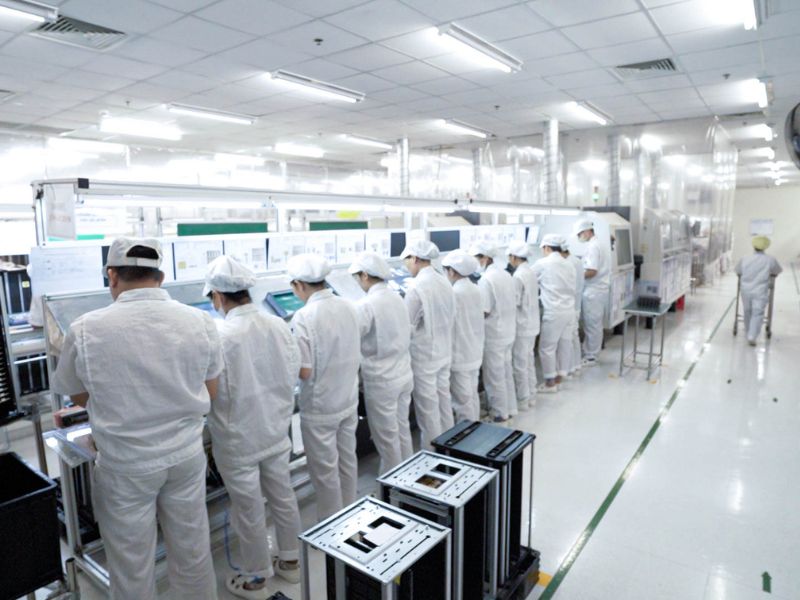
Before working with an EMS partner on DFT, OEMs should prepare:
- Product specification
- Schematic
- PCB layout
- Gerber files
- BOM
- Assembly drawing
- Test requirements
- Functional test procedure
- Firmware or programming instructions
- Mechanical files if fixture alignment is required
- Target production volume
- Quality requirements
- Failure criteria
- Traceability requirements
The more complete the test information, the easier it is for the EMS partner to recommend proper inspection, ICT, FCT, fixture planning, and quality control.
How DFT Supports Production Readiness
DFT is a key part of production readiness. A product is not truly ready for mass production if it cannot be tested consistently.
Good DFT helps OEMs:
- Confirm product quality at scale
- Reduce uncertainty during pilot production
- Improve failure analysis
- Support consistent quality records
- Optimize test cycle time
- Reduce manual inspection dependency
- Prepare for stable mass production
For OEMs moving from prototype to production, DFT should be reviewed together with BOM readiness, fixture readiness, sourcing readiness, and inspection planning.
How an EMS Partner Supports Design for Testability
An experienced EMS partner can review testability from a real production perspective. This is important because test access, fixture design, production flow, and quality control are not always obvious from the design side.
A capable EMS partner can help with:
- Test point review
- ICT feasibility review
- FCT procedure planning
- AOI and visual inspection review
- Fixture planning
- Firmware programming process
- Pilot run validation
- Failure analysis process
- Production test data control
This is one reason EMS provider selection should include testing capability, engineering support, quality systems, communication, and production experience—not only unit price.
Why Choose SHDC for DFT and PCBA Testing Support?
SHDC supports OEM customers with electronics manufacturing services, including SMT, DIP, assembly, testing, and packaging. For PCBA projects, SHDC’s production process can support key stages such as IQC inspection, SMT processing, reflow, AOI, component insertion, soldering, ICT, FCT, visual inspection, OQC, packaging, and finished goods handling.
This process-oriented capability is important for Design for Testability because DFT must connect PCB design with real inspection and testing conditions. A testable design should work not only in engineering review, but also on the production floor.
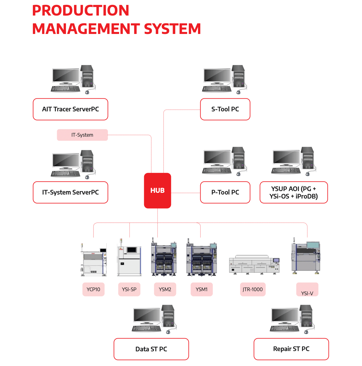
SHDC’s testing and inspection-related capabilities include AOI, ICT, functional testing, high-voltage testing, A/V testing, aging testing, and quality control processes. These capabilities help OEMs validate product quality before shipment and reduce avoidable production risks.
SHDC also supports PCBA applications such as chargers, power-related electronics, water purifier boards, computer mouse boards, petrol-related electronics, and automotive-related PCBA. For OEMs preparing products for pilot run or mass production, early DFT review can help improve test readiness and quality control.
For U.S. companies evaluating electronics manufacturing in Vietnam, SHDC can support projects from manufacturing review to PCBA production, testing, final assembly, and packaging. OEMs that need broader project support can also consider full-service EMS in Vietnam for integrated production support.
>>>Read more: Power Electronics Manufacturing in Vietnam – SHDC
Design for Testability for U.S. OEMs Working With Vietnam EMS Partners
For U.S. OEMs working with offshore EMS partners, clear test requirements are especially important. When engineering teams and production teams are in different countries, unclear test procedures can lead to delays, repeated questions, incorrect assumptions, and inconsistent quality expectations.
To improve collaboration, OEMs should:
- Share test requirements early
- Provide golden samples if available
- Define pass/fail criteria clearly
- Confirm firmware and programming needs
- Approve test fixtures before production
- Validate testing during pilot run
- Review test data and failure reports
- Align on retest and repair rules
- Confirm quality records and traceability requirements
DFT helps reduce communication risk because it turns testing expectations into documented design and production requirements.
Questions OEMs Should Ask Before PCBA Testing
Before moving to pilot run or mass production, OEMs should ask their EMS partner:
- What test method is suitable for this product?
- Is ICT required, or is FCT enough?
- Are test points sufficient?
- What test coverage can be achieved?
- Do we need a custom test fixture?
- How long will each test cycle take?
- How will failed units be handled?
- What test data will be recorded?
- Are firmware and programming steps included?
- What should be validated during pilot production?
- Are there any design changes that could improve testability?
These questions help OEMs evaluate whether the product is truly test-ready.
Final Thoughts
Design for Testability helps electronics OEMs make PCBAs easier to inspect, test, diagnose, and validate during production. It should be considered during PCB design, not after production files are finalized.
A strong DFT strategy includes test points, ICT access, FCT procedures, AOI visibility, firmware planning, fixture design, pass/fail criteria, and clear documentation. For OEMs preparing for pilot run or mass production, DFT reduces testing risk and improves production readiness.
If you are preparing a PCBA project for production, SHDC can help review your testing requirements and support manufacturing from SMT and DIP assembly to AOI, ICT, FCT, final inspection, and packaging.
FAQs About Design for Testability
What is Design for Testability in electronics?
Design for Testability in electronics is the process of designing a PCB or electronic product so it can be tested efficiently and reliably during production.
Why is DFT important for PCBA manufacturing?
DFT helps improve fault detection, reduce test time, support ICT and FCT, improve troubleshooting, and strengthen quality control before shipment.
What is the difference between DFM and DFT?
DFM focuses on making a product easier to manufacture, while DFT focuses on making it easier to test and verify during production. Both are important before pilot run and mass production.
What are PCB test points?
PCB test points are exposed pads or locations on a circuit board that allow test probes to access electrical signals during inspection, ICT, debugging, programming, or functional testing.
What files are needed for a DFT review?
Common files include schematic, PCB layout, Gerber files, BOM, assembly drawing, test point map, test procedure, firmware instructions, and pass/fail criteria.
Is ICT always required for PCBA testing?
No. ICT is useful for many products, especially complex or higher-volume PCBAs, but some products may rely on AOI, visual inspection, and FCT depending on complexity, cost, and quality requirements.
Can an EMS partner help with Design for Testability?
Yes. An EMS partner can review test point access, ICT feasibility, FCT requirements, fixture planning, inspection access, firmware programming, and production testing flow.