Tiếng Việt
 日本語
日本語Most engineers assume that production cost is determined on the factory floor. In reality, the decisions that drive manufacturing expense — yield loss, rework cycles, line stoppages, and design re-spins — are made weeks or months earlier, at a CAD workstation. Research consistently shows that approximately 70–80% of a product’s total manufacturing cost is locked in at the design phase, before a single component is ordered or a single board is fabricated. This is the problem that DFM for electronics manufacturing exists to solve. And for OEMs working with an EMS partner, DFM is not a software checkbox or a one-time review. It is the engineering discipline that bridges the gap between design intent and production reality — determining whether a product launches on yield, on schedule, and on cost, or enters an expensive cycle of rework and re-qualification. This guide covers what DFM for electronics manufacturing actually involves in a professional EMS context, the six-point DFM analysis framework that a qualified partner applies, where most programs fail, and what to demand from your manufacturer before the first board is built.
What Is DFM for Electronics Manufacturing?
DFM for electronics manufacturing is not a checklist. It is a philosophy of concurrent engineering — one that requires designers and manufacturing partners to share the same set of constraints from the project’s earliest stages.
DFM Defined: Beyond the Textbook
Design for Manufacturability (DFM) is the systematic process of reviewing and optimizing a PCB design so that it can be fabricated, assembled, tested, and scaled reliably and economically using standard production processes.
At the technical level, DFM for electronics manufacturing integrates two complementary disciplines:
- DFF (Design for Fabrication): Ensuring the bare board can be reliably etched, drilled, and laminated within the physical tolerances of the production facility — trace widths, clearances, annular ring sizes, via aspect ratios, layer stackup compatibility.
- DFA (Design for Assembly): Ensuring that components can be placed, soldered, and inspected efficiently by automated machinery — component spacing, pad geometry, thermal relief, stencil aperture compatibility, orientation standardization.
A board that passes electrical design rule checks but ignores DFF and DFA principles may function perfectly in simulation and fail repeatedly on the production line.
DFM vs. DFT vs. DFA: Understanding the Full Scope
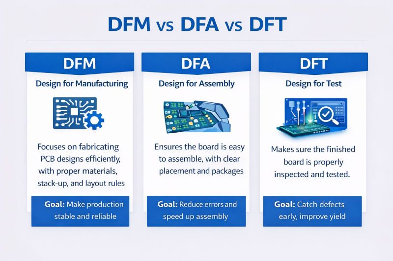
| Discipline | Full Name | Primary Question | Handled By |
|---|---|---|---|
| DFM | Design for Manufacturability | Can this be built reliably at scale? | EMS process engineers |
| DFT | Design for Testability | Can every defect be detected efficiently? | Test engineers |
| DFA | Design for Assembly | Can components be placed and soldered by automated equipment? | SMT process engineers |
| DFF | Design for Fabrication | Can the bare board be fabricated within process capability? | PCB fabrication team |
In a professional EMS environment, all four disciplines are applied simultaneously as part of a unified DFM analysis — not sequentially.
DFM vs. Standard Prototype Review
A standard prototype review asks: “Does this design work?”
DFM for electronics manufacturing asks a fundamentally different set of questions:
- Can this design be built consistently at volume without manual intervention?
- Will it yield above target with standard automated processes?
- Can every defect be detected before the board leaves the production line?
- Is the supply chain qualified and stable enough to support ramp?
These are manufacturing questions, not design questions. Answering them requires a different set of skills, tools, and processes — and they must be answered before the first build, not discovered during it.
Understanding what PCBA manufacturing involves is the foundation — DFM is where that knowledge is applied under real production constraints.
Why DFM for Electronics Manufacturing Matters: The Real Cost of Skipping It
The financial case for DFM in electronics manufacturing is not theoretical. It is built on a simple, well-documented principle: the cost of fixing a design or process error escalates dramatically as a program progresses.
The Cost Escalation Curve
| Stage Error Is Discovered | Relative Cost to Fix | Typical Impact |
|---|---|---|
| Design / DFM review | 1× | Engineering hours only |
| Prototype build (EVT) | 10× | Rebuild cost + schedule delay |
| Pilot run (PVT) | 100× | Scrap + fixture rework + ramp delay |
| Mass production (MP) | 1,000× | Line stoppage + customer penalty + potential recall |
This cost multiplier model is why leading OEMs treat DFM review as a non-negotiable gate — not an optional service.
A real-world example from Siemens EDA illustrates the stakes clearly: a PCB initially yielding a 25% success rate was redesigned in adherence to IPC design rules without changing any components. The result: yield increased to 88%. The fix cost engineering hours. Discovering the same issues at mass production would have cost orders of magnitude more.
The 6 Most Common DFM Failures in Electronics Manufacturing
DFM for electronics manufacturing consistently catches the same failure modes across product types and industries. These six issues account for the majority of yield losses in programs that skip a formal DFM analysis:
1. Fine-pitch component clearance violations Components placed too close together prevent automated pick-and-place machines from achieving reliable placement. Result: systematic misalignment defects across every board in the production run. Component placement is consistently one of the top failure points in DFM for electronics manufacturing — and the cheapest to fix at design stage.
2. Via-in-pad without proper copper fill Vias placed directly under BGA or QFN pads cause solder to wick into the via during reflow, creating voids and unreliable solder joints. This defect is invisible to AOI and requires X-ray inspection to detect.
3. Insufficient ICT test point access Test points that are too small, too closely pitched, or inaccessible to a bed-of-nails fixture reduce ICT coverage below acceptable thresholds. Defects that escape ICT reach the field — generating warranty costs that dwarf the cost of a DFT review.
4. Stencil aperture area ratio below 0.66 Apertures with an area ratio below 0.66 produce inconsistent solder paste release — the root cause of insufficient solder, bridging, and tombstoning defects. This is a stencil design issue that DFM analysis catches before the first print cycle.
5. Single-source BOM components Components available from only one manufacturer create supply chain fragility. At MP ramp, a single supplier shortage can halt production for weeks. DFM BOM scrubbing identifies these risks and qualifies alternates before they become crises.
6. Non-standard panel design Boards panelized without proper rail clearances, fiducial markers, or breakout tab geometry cause conveyor handling damage and placement registration errors across the entire production run.
What the Data Shows
- 70–80% of total manufacturing cost is determined at the design phase — making DFM for electronics manufacturing the highest-leverage cost control activity in the product lifecycle
- 70% of PCB jobs may be put on hold due to incorrect documentation or unmanufacturable design data
- Tolerance optimization alone can reduce piece-part costs by 20–50% in applications where tolerances were previously over-specified
- First-pass yield, rework rate, production delays, and assembly defects are all measurably improved when DFM PCB assembly guidelines are applied correctly from the start
For OEMs considering offshore PCB assembly, understanding offshore manufacturing risks — many of which trace back to inadequate DFM — is essential before selecting a partner.
The EMS Partner’s DFM Analysis Process: What Actually Happens
A professional approach to DFM for electronics manufacturing does not begin with a verbal review or a courtesy check. It is a structured, documented engineering process with defined inputs, a formal six-point DFM analysis framework, and a written output that the OEM can act on immediately.
What to Send Your EMS Partner: The DFM Input Package
Before any DFM review can begin, the following design package is required:
- Gerber files (RS-274X format, all layers including drill, silkscreen, solder mask)
- BOM with manufacturer part numbers (MPN), manufacturer name, and packaging format
- Assembly drawings (top and bottom, with component orientation and reference designators)
- Schematic (for DFT review — net connectivity verification)
- IPC class requirement (Class 2 for commercial/industrial, Class 3 for medical/automotive)
- Target yield and volume forecast (process capability requirements scale with volume)
- Special requirements (conformal coating, underfill, press-fit connectors, controlled impedance)
Incomplete design packages are the single most common cause of DFM review delays. A qualified EMS partner defines these requirements clearly at project kickoff — not after the first review cycle has already been delayed.
The 6-Point DFM Analysis Framework
This is the core of what a professional EMS engineering team does before your first board is built. Each point in the DFM for electronics manufacturing review addresses a distinct category of production risk.
Point 1 — Component Placement Review
The placement review verifies that every component on the board can be placed, soldered, and inspected by automated production equipment without manual intervention — a foundational requirement of any DFM PCB assembly process.
Key checks performed:
- Minimum clearance between components — verified against IPC-7351 land pattern standards and the specific equipment capabilities of the production line
- Orientation consistency — polarized components (capacitors, diodes, ICs) reviewed for consistent orientation to reduce placement errors and enable efficient AOI programming
- Keep-out zones — component-free areas around board edges (minimum 3mm for conveyor rails), mounting holes, and connector areas
- Component height restrictions — maximum height verified against enclosure clearances and conformal coating nozzle access
- Fine-pitch and BGA placement — clearance to adjacent components verified for rework access; underfill dispensing clearance confirmed where required
The SMT assembly process places components at speeds up to 95,000 CPH — but only when the layout supports automated handling. Placement violations discovered at this stage of DFM for electronics manufacturing cost engineering hours to fix. Discovered during a pilot run, they cost weeks.
Point 2 — Solder Paste & Stencil Analysis
The stencil analysis determines whether the solder paste printing process can reliably deposit the correct volume of paste on every pad — the foundation of solder joint quality for every SMT component on the board. This is one of the most impactful elements of a thorough DFM analysis.
Key checks performed:
- Aperture area ratio — minimum 0.66 required for reliable paste release; fine-pitch pads below this threshold require step-stencil design
- Aperture geometry optimization — rectangular vs. home-plate apertures for fine-pitch components; reduced apertures for via-in-pad designs
- Step-stencil requirements — identified for boards with mixed component heights
- Paste volume balance — large pads adjacent to small pads reviewed for paste volume consistency
- Solder mask dam adequacy — minimum solder mask width between adjacent pads verified to prevent bridging
Stencil design issues caught at DFM review stage cost a stencil revision. Caught after the first pilot build, they cost a full production run of scrap and a 2–3 week delay.
Point 3 — PCB Stack-up & Trace Review
The trace and stack-up review verifies that the bare board design is manufacturable within standard fabrication process capabilities — a core element of manufacturability guidelines for any PCB design.
Key checks performed:
- Trace width vs. current capacity — minimum trace widths verified against IPC-2221 current-carrying capacity tables
- Minimum trace/space rules — verified against fabricator capability (standard: 4/4 mil; advanced: 3/3 mil; HDI: 2/2 mil or below)
- Via aspect ratio — depth-to-diameter ratio verified for reliable copper plating (maximum 10:1 for standard through-hole vias)
- Copper balance — copper distribution across layers reviewed for warpage risk during reflow; unbalanced copper on outer layers is a leading cause of board warpage in DFM for electronics manufacturing programs
- Impedance-controlled traces — stack-up verified against impedance targets; tolerance requirements communicated to fabricator
- Annular ring adequacy — minimum annular ring verified to survive drill registration tolerances without creating open circuits
Point 4 — Thermal Management Review
Thermal management review verifies that the board design supports reliable soldering of all components and that no component will exceed its rated junction temperature — a critical DFM analysis step for power-dense designs.
Key checks performed:
- Reflow profile compatibility — component temperature ratings verified against the reflow profile required by the solder paste and board thermal mass; mixed-technology boards with heat-sensitive components reviewed for thermal exposure
- Thermal relief design — through-hole component pads on internal power planes reviewed for thermal relief spoke design; insufficient thermal relief causes cold solder joints on wave solder
- Power component placement — high-dissipation components reviewed for placement relative to board thermal mass and adjacent heat-sensitive components
- Thermal via design — thermal via arrays under power pads (QFN, DPAK, D2PAK) reviewed for via count, diameter, and fill specification to ensure adequate heat transfer
For high-power applications — including GaN power electronics — thermal management is one of the most technically demanding aspects of DFM for electronics manufacturing. See power electronics manufacturing in Vietnam for how SHDC approaches thermal DFM for GaN fast charger designs.
Point 5 — Testability Review (DFT)
The DFT review determines whether every manufacturing defect that can occur on the board can be detected efficiently by the production test strategy — a non-negotiable element of DFM PCB assembly for any product with field reliability requirements.
Key checks performed:
- ICT test point coverage — every net reviewed for test point accessibility; minimum test point diameter 1.0mm; minimum pitch 2.54mm (1.27mm for high-density)
- Test coverage calculation — percentage of nets covered by ICT calculated and reported; target ≥85% for commercial, ≥95% for industrial/medical
- Test point placement — test points verified to be on the bottom side of the board for bed-of-nails fixture access
- Functional test interface — connector and test pad placement reviewed for FCT jig access
- BGA and hidden joint testability — nets connected only to BGA or QFN hidden joints flagged for boundary scan or X-ray inspection requirement
ICT fixture development takes 4–8 weeks. The DFT review within the DFM for electronics manufacturing process must happen at design stage — not after DVT — to ensure test infrastructure is ready when the pilot run completes.
For a detailed explanation of how ICT and functional testing work in production, see in-circuit testing (ICT) and PCBA testing.
Point 6 — BOM & Supply Chain Review
The BOM review is the supply chain risk assessment component of DFM for electronics manufacturing — verifying that every component specified in the design can be sourced reliably at the volumes and lead times required for production ramp.
Key checks performed:
- Lead time verification — every component checked against current distributor stock and lead time; long-lead items (>12 weeks) flagged for early ordering
- EOL (End-of-Life) flags — components approaching manufacturer discontinuation identified; recommended replacements sourced and specified
- Single-source risk — components available from only one manufacturer identified; second-source alternates qualified and added to BOM
- Packaging format — all components verified to be available in tape-and-reel for automated placement; cut-tape and tray components flagged for feeder setup impact
- Component standardization — non-standard footprints, unusual packages, and obsolete component types identified with replacement recommendations
- Moisture sensitivity level (MSL) — MSL ratings for all ICs verified; baking and dry storage requirements documented for production floor
BOM issues discovered at pilot stage — particularly long-lead shortages — are the most common cause of MP ramp delays. A thorough BOM review as part of DFM analysis at design stage, with early orders placed for long-lead items, eliminates this risk entirely.
The DFM Report: What a Professional Output Looks Like

A professional DFM review output is not a verbal briefing or a list of bullet points in an email. It is a structured engineering document that the OEM can act on immediately.
Standard DFM report structure:
| Section | Content |
|---|---|
| Executive Summary | Total findings by severity; overall DFM risk rating |
| Critical Findings | Issues that will cause production failure — must fix before any build |
| Major Findings | Issues that will cause yield loss — should fix before pilot run |
| Minor Findings | Recommended improvements for future revision |
| BOM Status | Lead time summary, EOL flags, single-source risks, alternates |
| DFT Coverage Report | ICT coverage %, uncovered nets, recommended test point additions |
| Process Recommendations | Stencil spec, reflow profile notes, assembly sequence |
Turnaround time: 24–48 hours for standard complexity boards (≤200 components); 3–5 business days for complex boards (BGAs, fine-pitch ICs, mixed technology).
Every finding includes: location reference, description of the issue, root cause, recommended fix, and estimated cost impact if not addressed. This level of documentation is what separates a professional DFM for electronics manufacturing service from a basic pre-production check.
DFM for Electronics Manufacturing Across the Product Lifecycle
DFM for electronics manufacturing is most powerful when applied early — but it remains relevant and valuable at every stage of the product lifecycle, from first prototype through sustained mass production.
DFM at Each NPI Stage
| NPI Stage | DFM Activity | Primary Benefit |
|---|---|---|
| Pre-EVT | Full DFM + DFT review | Catch all issues before any build cost is committed |
| EVT | Build issues log → design update | Validate fixes before DVT process development |
| DVT | Process parameter validation | Lock stencil spec, reflow profile, placement offsets |
| PVT | Yield data → process optimization | Confirm DFM effectiveness at production volume |
| MP | Control Plan enforcement | Sustain yield through the production lifetime |
The relationship between DFM for electronics manufacturing and NPI is inseparable. For a complete guide to the NPI process — from EVT through mass production ramp — see NPI in electronics manufacturing.
DFM for New Designs vs. Redesigns vs. Transfer Products
New design: Full DFM analysis from scratch — highest leverage point in the entire product lifecycle. Every finding caught here saves 10–1,000× the cost of discovering it later.
Redesign (ECO): Targeted DFM on changed areas, plus impact assessment on unchanged areas that may be affected by the change. A component substitution that appears minor can change the reflow profile requirement for adjacent components.
Transfer product: Full DFM for electronics manufacturing re-review is mandatory when moving production from one EMS to another. Process assumptions from the previous manufacturer — stencil specifications, reflow profiles, placement offsets, test programs — do not automatically transfer. A transfer product that arrives without a DFM re-review frequently experiences yield regression at the new facility.
For OEMs evaluating contract PCB assembly options or considering a China alternative for their manufacturing base, DFM re-review at transfer is a non-negotiable requirement for maintaining yield continuity.
DFM for Electronics Manufacturing by Product Type: Special Considerations
Different product categories present distinct challenges in DFM for electronics manufacturing. A professional EMS partner applies product-type-specific DFM knowledge — not a generic checklist — to each program.
DFM for High-Density / Fine-Pitch Boards
High-density boards with 0402, 0201, or 03015 components and fine-pitch ICs require DFM analysis at every level:
- Stencil aperture design is critical — area ratios below 0.66 are common on 0201 pads and require step-stencil or nano-coating solutions
- BGA underfill requirements must be specified in the DFM report — underfill dispensing clearance from adjacent components is a common oversight in DFM PCB assembly for high-density boards
- X-ray inspection requirement for hidden solder joints (BGA, QFN, LGA) must be identified at DFM stage so inspection infrastructure is in place before pilot builds
DFM for Mixed-Technology Boards (SMT + Through-Hole)
Mixed-technology boards require careful DFM for electronics manufacturing attention to assembly sequence and thermal management:
- Assembly sequence optimization: SMT components are placed and reflowed first; through-hole components are added and wave-soldered or selectively soldered second. DFM verifies that SMT components on the bottom side are positioned to survive wave solder exposure.
- Wave solder vs. selective solder decision: DFM analysis identifies which through-hole components require selective soldering and which can be wave-soldered efficiently
- Solder mask requirements: SMT components exposed to wave solder require solder mask protection — DFM verifies coverage is adequate
For a detailed comparison of assembly methods, see SMT vs. through-hole assembly and wave soldering vs. reflow soldering.
DFM for High-Power / GaN Electronics
GaN power electronics represent one of the most demanding DFM for electronics manufacturing challenges in consumer and industrial electronics:
- Thermal via design for power dissipation under GaN FETs and power ICs: via count, diameter, and copper fill specification must be optimized to achieve junction temperatures within rated limits
- Creepage and clearance for high-voltage traces: IPC-2221 spacing requirements for the operating voltage must be verified across the entire board
- Component placement for thermal symmetry: heat-generating components must be distributed to prevent localized thermal stress that causes board warpage during reflow
See GaN charger manufacturing in Vietnam for how SHDC applies high-power DFM analysis to GaN fast charger production.
DFM for Medical and Automotive PCBA
Medical and automotive electronics require DFM for electronics manufacturing aligned to the most stringent quality standards in the industry:
- IPC Class 3 requirements impose tighter acceptance criteria — DFM must verify that the design supports Class 3 inspection without excessive rework
- Traceability requirements begin at the design stage: component lot traceability, board serial number placement, and DHR compatibility must be designed in, not added later
- PPAP documentation for automotive programs requires DFM to be documented as part of the Process FMEA and Control Plan
For IPC standards compliance requirements and their DFM implications, see SHDC’s guide to IPC-A-610 and J-STD-001. For medical device requirements, see medical device electronics manufacturing Vietnam and ISO 13485.
DFM Checklist: What to Demand From Your EMS Partner
Before awarding a program to a contract manufacturer, use this DFM checklist as a minimum qualification filter. An EMS partner who cannot confirm these capabilities should not be managing your product’s path to production.
DFM for Electronics Manufacturing — Partner Evaluation Checklist
Design Review
- Formal written DFM report provided before first build — not verbal feedback
- DFT (Design for Testability) review included in DFM scope
- Gerber and schematic review by a qualified process engineer
- IPC class requirement confirmed and applied to review criteria
- Findings classified by severity: Critical / Major / Minor
- Cost impact estimate provided for each critical finding
Supply Chain
- Full BOM lead time check with current distributor data
- EOL component flags with recommended replacements
- Single-source risk identification with alternate component qualification
- Packaging format verification (tape-and-reel availability confirmed)
- MSL rating documentation for all moisture-sensitive devices
Process Validation
- Stencil aperture specification included in DFM output
- Reflow profile compatibility verified for all components
- Wave/selective solder requirements identified for through-hole components
- Thermal management review for power components
- Assembly sequence defined for mixed-technology boards
Test Infrastructure
- ICT test coverage percentage calculated and reported
- Uncovered nets identified with recommended test point additions
- ICT fixture development timeline agreed at project kickoff
- FCT jig requirements identified and timeline confirmed
- X-ray inspection requirement identified for hidden solder joints
For a broader EMS partner evaluation framework, see electronics supplier due diligence and electronics factory audit checklist.
DFM for Electronics Manufacturing at SHDC: Engineering-Led, Production-Proven

SHDC Electronics is a full-service EMS provider located in the Vietnam Singapore Industrial Park — Hai Duong (VSIP Hai Duong), 40km from Hanoi and 55km from Haiphong Port. With a 2,600 m² facility, 150 employees, and a dedicated Engineering Department comprising both Product Technical and Technical Factory teams, SHDC treats DFM for electronics manufacturing as a distinct engineering discipline — not a pre-sales activity or a courtesy review.
Engineering Infrastructure That Makes DFM Actionable
Yamaha Smart Factory Integration
SHDC’s DFM analysis process is backed by Yamaha’s production management ecosystem: S-Tool PC and P-Tool PC for process simulation and program development before the first build; YSUP / iProDB for production data management; and YSI-OS for AOI program management.
This means DFM recommendations are not theoretical — they are validated against the actual process capabilities of the production equipment that will build your product. Process parameters developed during DFM review are directly transferable to the production line — no re-programming, no re-calibration, no yield regression at ramp.
3D SPI and 3D AOI from Prototype Stage
The Yamaha YSI-SP 3D Solder Paste Inspection system validates stencil design before the first reflow cycle — a direct extension of the stencil analysis performed during DFM for electronics manufacturing review. If paste volume is outside specification on specific apertures, the stencil is corrected before any components are placed, saving an entire build cycle.
The Yamaha YSI-V 3D AOI system is active from the first prototype build. AOI data from prototype and DVT builds defines the inspection program for PVT and mass production — creating a validated, data-backed inspection baseline.
See automated optical inspection (AOI) for a detailed explanation of how 3D AOI works in SHDC’s production environment.
Precision Placement Capability
| Equipment | Placement Accuracy | Speed | Component Range |
|---|---|---|---|
| Yamaha YSM20R | ±0.03mm (Cpk ≥ 1.00) | 95,000 CPH | 0402 to 32×32mm |
| Yamaha YSM10 | ±0.035mm | 46,000 CPH | 03015 to 55×100mm |
| Yamaha YCP10 | Screen printer | 1–200mm/sec | 0.4–3.0mm board thickness |
The same equipment used for DFM PCB assembly validation builds is the production equipment — ensuring that yield data from prototype and pilot builds is directly predictive of mass production performance.
ICT and Functional Testing
The Kyoritsu ICT F-2000 Plus provides parametric in-circuit test capability. Dedicated FCT stations, aging test equipment, high-voltage test, and AV test infrastructure support comprehensive functional validation from prototype through mass production.
ICT fixture development is initiated at DVT stage — not after PVT — ensuring test infrastructure is ready when the pilot run completes. This is one of the most common sources of NPI delay at EMS providers who treat test development as an afterthought to DFM for electronics manufacturing.
Digital Management System
SHDC operates an integrated ERP / PLM / SCM / MES / QMS digital infrastructure. The AIT Tracer system provides board-level traceability from the first pilot build. According to SHDC’s production management data, this integration reduces decision-making time by 30% and reduces defective inventory by 30% — outcomes that are particularly valuable during the high-iteration DFM analysis and NPI phase.
Proven Across Demanding Product Categories

GaN Power Electronics SHDC has successfully executed DFM for electronics manufacturing and production for a full range of GaN fast chargers — 65W, 67W, 70W Slim, 100W 2C2A, 102W, 120W (including Bluetooth-enabled), and 150W 3C1A configurations. GaN power electronics represent one of the most demanding DFM challenges in consumer electronics: high-density layouts, tight thermal constraints, and stringent electrical safety requirements.
Automotive PCBA — Thaco DFM analysis for Thaco automotive PCBA was conducted under PPAP-level documentation requirements — the most rigorous DFM documentation standard in manufacturing. Full Control Plan, PFMEA, and component traceability documentation were produced as part of the DFM deliverable. See automotive PCBA Vietnam.
Medical Device Electronics For OEMs requiring ISO 13485-aligned DFM for electronics manufacturing processes — including full component traceability from prototype stage, documented process validation, and DHR-compatible build records — SHDC’s quality infrastructure supports medical device DFM requirements. See medical device electronics manufacturing Vietnam.
Industrial and Commercial Electronics DFM review programs for PECO industrial electronics, Karofi/Tecomen water purifier control boards, and computer peripherals have demonstrated SHDC’s ability to apply DFM across diverse product types and complexity levels. See industrial electronics manufacturing in Vietnam.
Phase 2 Expansion — March 2027
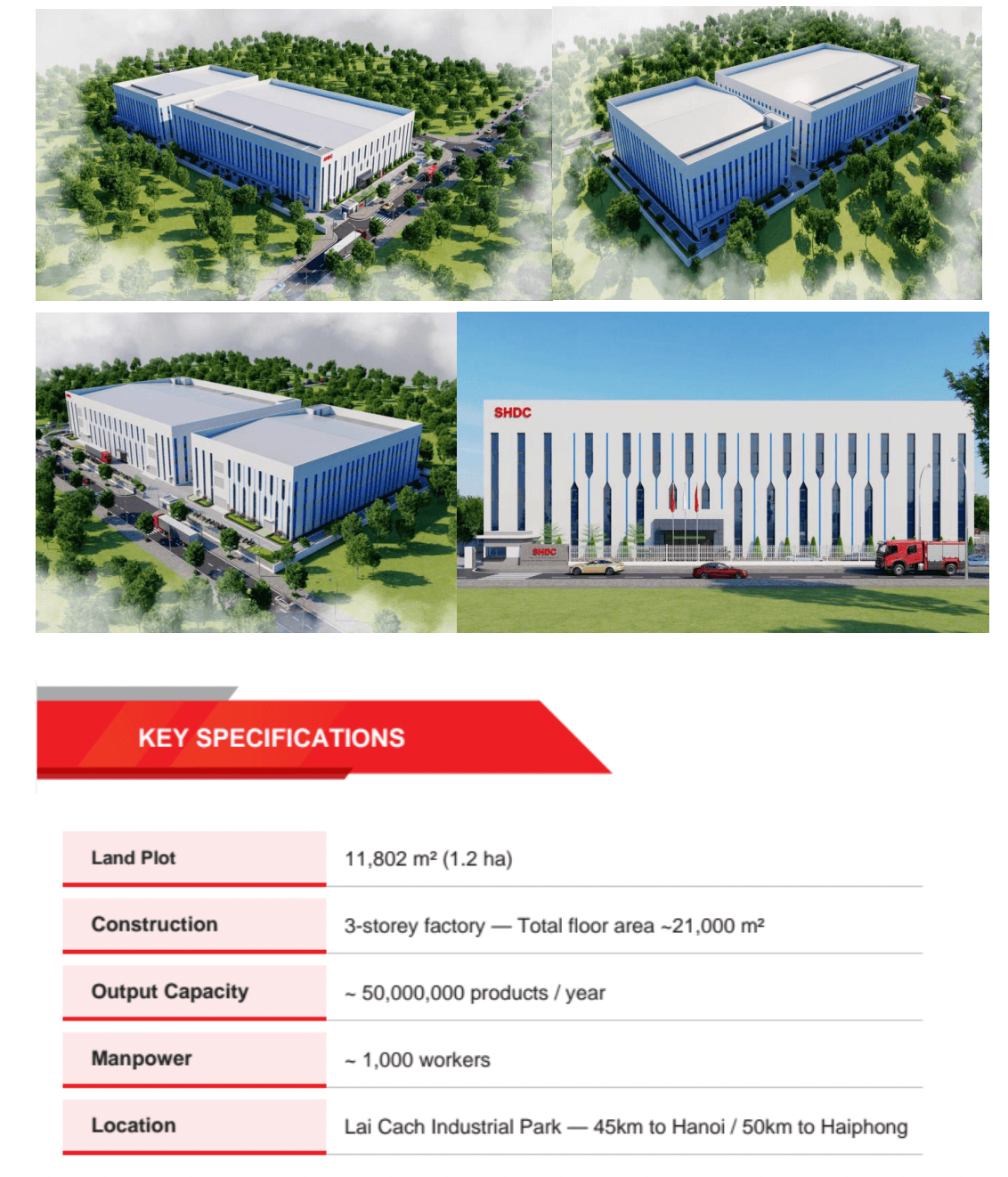
SHDC’s new facility at Lai Cach Industrial Park will add 10 SMT lines, 8 DIP lines, 10 assembly lines, and full inline ICT/FCT/AOI 3D capability — scaling DFM for electronics manufacturing and production capacity to support 50M units/year. DFM programs started today will have a clear, validated path to high-volume production within the same manufacturing ecosystem.
For OEMs evaluating Vietnam as a manufacturing base, see why Vietnam is the top choice for electronics manufacturing in 2026 and 10 reasons to choose contract electronics manufacturing in Vietnam.
Frequently Asked Questions
What is DFM for electronics manufacturing?
DFM for electronics manufacturing (Design for Manufacturability) is the systematic process of reviewing and optimizing a PCB design so that it can be fabricated, assembled, tested, and scaled reliably and economically using standard production processes. It encompasses design for fabrication (DFF), design for assembly (DFA), and design for testability (DFT) — applied simultaneously before the first physical build.
What does a DFM analysis include?
A professional DFM analysis includes six core review areas: component placement, solder paste and stencil specification, PCB stack-up and trace review, thermal management assessment, testability (DFT) review, and BOM/supply chain scrubbing. The output is a written report classifying all findings by severity — Critical, Major, and Minor — with recommended fixes and cost impact estimates.
When should DFM for electronics manufacturing be performed?
DFM for electronics manufacturing should be performed before the first physical build — ideally when the design is at 90–95% completion. This is the highest-leverage point in the product lifecycle: every issue caught at DFM stage costs engineering hours to fix; the same issue discovered at pilot run costs weeks and significant scrap.
What is the difference between DFM and DFT?
DFM (Design for Manufacturability) focuses on whether the design can be built reliably and economically by automated production processes. DFT (Design for Testability) focuses on whether every manufacturing defect that can occur can be detected efficiently by the production test strategy (ICT, FCT, AOI). In a professional EMS environment, both are performed simultaneously as part of the unified DFM for electronics manufacturing review.
How does DFM for electronics manufacturing reduce PCB cost?
DFM for electronics manufacturing reduces cost through four mechanisms: (1) preventing design re-spins by catching issues before tooling is committed; (2) improving first-pass yield by eliminating systematic defect sources; (3) reducing rework labor by eliminating assembly process problems; (4) stabilizing the supply chain by qualifying alternate components before shortages occur. Research shows 70–80% of total manufacturing cost is determined at the design phase — DFM analysis is the discipline that optimizes those decisions.
Can DFM be applied to an existing design or only new designs?
DFM for electronics manufacturing applies to new designs, redesigns (ECOs), and transfer products moving from another EMS provider. Transfer products in particular require a full DFM re-review — process assumptions from the previous manufacturer do not automatically transfer, and yield regression at transfer is common without a re-review.
What file formats are needed for a DFM review?
Standard DFM review input package: Gerber files (RS-274X), drill files (Excellon), BOM with manufacturer part numbers, assembly drawings, schematic (for DFT review), pick-and-place data, and IPC class specification.
What should I look for in an EMS partner for DFM?
Key indicators of genuine DFM for electronics manufacturing capability: formal written DFM report before first build (not verbal feedback), DFT coverage report included, BOM scrubbing with lead time and EOL data, findings classified by severity with cost impact estimates, and ICT fixture development timeline agreed at project kickoff — not after DVT.
Conclusion
The engineering quality of a PCB design’s path from Gerber files to production floor — governed by a rigorous DFM for electronics manufacturing process — determines its commercial viability as much as the circuit design itself. A product that enters production with a validated DFM analysis behind it runs at target yield, ships on schedule, and generates the margins the business model requires. A product that skips DFM enters production with unknown process risks — and pays for that decision in scrap, rework, and schedule delays that compound at every stage.
The regulatory trajectory for electronics manufacturing — particularly in medical, automotive, and industrial segments — is making structured DFM for electronics manufacturing not just a competitive advantage but a compliance requirement. Process validation documentation, traceability from prototype stage, and PFMEA-backed Control Plans are increasingly demanded by OEM customers as conditions of supply.
The right EMS partner for DFM PCB assembly doesn’t just review your Gerber files — they engineer the path from your design to a scalable, documented, auditable production process.