
 Tiếng Việt
 日本語
日本語
Most hardware product delays don’t happen in the R&D lab — they happen in the gap between a validated prototype and a stable production line. A design that works perfectly on an engineer’s bench can fail repeatedly on a production floor, generating scrap, delaying shipments, and eroding the margins that made the product viable in the first place. This gap has a name: New Product Introduction (NPI). And how well it is managed determines whether a product launches on time, on yield, and on cost — or spends months in an expensive cycle of rework and re-qualification. NPI in electronics manufacturing is not a single build — it is a structured, multi-phase engineering process that transforms a validated design into a repeatable, scalable production system. This guide covers what NPI actually involves, the five phases from first prototype to mass production, where most programs fail, and what to demand from an EMS partner before you hand over your design files.
What Is NPI in Electronics Manufacturing?
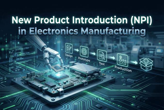
NPI — New Product Introduction — is the end-to-end process of taking a new or redesigned electronic product from its first physical build through to a stable, high-yield mass production state. It is not simply “building a prototype.” It is the engineering discipline of making a design manufacturable, testable, and scalable.
NPI vs. Prototype: Understanding the Difference
A prototype answers the question: “Does this design work?”
NPI answers a different set of questions:
- Can this design be built consistently at volume?
- Can it be tested efficiently on a production line?
- Will it yield above target with standard production processes?
- Is the supply chain qualified and ready to support ramp?
These are manufacturing questions, not design questions — and they require a different set of skills, tools, and processes to answer.
The Four Build Stages Within NPI
| Stage | Full Name | Primary Question | Typical Volume |
|---|---|---|---|
| EVT | Engineering Validation Test | Does the design work as intended? | 5–20 units |
| DVT | Design Validation Test | Does the design meet all specifications with production-intent processes? | 20–50 units |
| PVT | Production Validation Test | Is the production process stable and repeatable? | 100–500 units |
| MP | Mass Production | Ongoing production at target volume and yield | Per forecast |
NPI encompasses the full journey from EVT through PVT — and the quality of that journey determines the health of MP.
Why NPI Fails Without a Structured Process
The cost of fixing a design or process error escalates dramatically as a program progresses:
- At design stage: Cost = engineering hours
- At EVT/DVT stage: Cost = prototype builds + engineering iteration
- At PVT stage: Cost = pilot run scrap + fixture rework + schedule delay
- At MP stage: Cost = production line downtime + customer delivery failure + potential recall
Research consistently shows that the majority of product launch delays trace back to inadequate NPI planning — specifically, DFM issues discovered too late, BOM errors that surface at pilot stage, and test strategies defined after tooling is already committed.
Understanding what PCBA manufacturing involves is the foundation — but NPI is where that knowledge is applied under real production constraints.
The 5-Phase NPI Process: From First Prototype to Mass Production
A well-executed NPI process follows a defined sequence of phases, each with specific inputs, activities, outputs, and go/no-go criteria. Skipping or compressing any phase doesn’t save time — it transfers risk forward into a more expensive stage.
Phase 1 — Design Review & DFM Analysis (Pre-NPI Gate)
Before a single component is placed, a qualified EMS partner reviews the complete design package against the realities of production. This is the highest-leverage activity in the entire NPI process.
What happens:
DFM (Design for Manufacturability) Review The EMS engineering team reviews Gerber files, BOM, schematic, and assembly drawings to identify features that will cause production problems:
- Fine-pitch components below the process capability of the production line
- Via-in-pad designs requiring special solder paste management
- Insufficient component clearances for automated placement
- Non-standard component footprints that require manual assembly
- Board edge clearances that conflict with conveyor rail dimensions
- Mixed-technology designs requiring multiple assembly passes
DFT (Design for Testability) Review
- Are ICT test points accessible and correctly sized?
- Is test coverage adequate for the product’s quality requirements?
- Are functional test interfaces defined and accessible?
- Can the board be fixtured for automated testing?
BOM Scrubbing
- Component availability check: are all parts in stock or on short lead time?
- EOL (End-of-Life) flag: are any components approaching discontinuation?
- Single-source risk: are critical components available from multiple suppliers?
- Packaging format: are all components available in tape-and-reel for automated placement?
- Approved alternates: are second-source components identified for long-lead items?
Output: A formal DFM report with prioritized findings — critical (must fix before build), major (should fix before pilot), and minor (recommended for future revision).
Every DFM issue caught at this stage saves 10–100x the cost of discovering it after tooling and pilot builds are committed. This is why prototype PCBA manufacturing done right always begins with engineering review, not a build.
Phase 2 — Prototype Build (EVT — Engineering Validation Test)
The first physical build answers one question: does the design work as the engineers intended? At this stage, manufacturing efficiency is secondary to speed of feedback.
What happens:
- First build of 5–20 units, typically with some manual assembly acceptable
- Engineering team documents every build challenge: component orientation issues, footprint mismatches, assembly sequence problems
- Bench testing by OEM engineering team: functional verification, electrical characterization, environmental stress screening
- First-pass yield data recorded — even at low volume, yield data reveals systematic issues
Common issues discovered at EVT:
- Schematic errors (incorrect component values, missing pull-up/pull-down resistors)
- Component orientation errors in the design files
- Thermal management problems (components running hot under load)
- EMI/EMC issues that weren’t apparent in simulation
- Mechanical interference between components and enclosure
Output:
- Build issues log with root cause analysis
- Component fit/form/function verification report
- Initial test results and failure analysis
- List of design changes required before DVT
Understanding the SMT assembly process and DIP assembly at this stage helps engineering teams anticipate which design features will create assembly challenges.
Phase 3 — Design Iteration & Process Development (DVT — Design Validation Test)
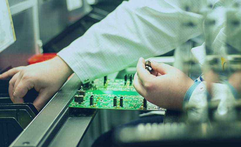
DVT is where the design is finalized and the production process is defined. This is the most engineering-intensive phase of NPI — and the one most commonly under-resourced.
What happens:
Design Changes Implemented All critical and major DFM findings from EVT are incorporated into the design. Updated Gerber files, BOM, and assembly drawings are released.
Process Parameter Definition
- Reflow profile developed and validated: preheat ramp rate, peak temperature, time above liquidus, cooling rate — all optimized for the specific component mix and board thermal mass
- Stencil design finalized: aperture geometry, area ratio, and step-stencil requirements for mixed-height components
- Wave solder / selective solder parameters defined: flux type, preheat temperature, solder bath temperature, conveyor speed, dwell time
- Placement offsets calibrated for each component type on the production equipment
Test Infrastructure Development
- ICT bed-of-nails fixture design initiated — this takes 4–8 weeks and must start at DVT, not PVT
- FCT (Functional Test) jig design and build
- Test program development and debug
- AOI programming for the specific board layout
DVT Build
- 20–50 units built using production-intent processes — no manual workarounds
- All process parameters documented and applied consistently
- First yield data from production-intent process collected by step
Output:
- Locked process parameters (reflow profile, stencil spec, placement offsets)
- Validated test fixtures (or fixtures in final build/debug)
- Updated BOM with approved alternates and packaging specifications
- DVT yield data and failure analysis
The PCBA manufacturing process at DVT stage is where the production Control Plan begins to take shape — defining inspection criteria, process controls, and quality checkpoints for every step.
Phase 4 — Pilot Run (PVT — Production Validation Test)
PVT is the critical gate between NPI and mass production. The question shifts from “does the design work?” to “is the production process stable, repeatable, and capable of meeting yield targets at volume?”
What happens:
- First run on the actual production line — 100–500 units
- All production processes active: no manual workarounds, no engineering interventions
- Full traceability active: every board carries a serial number, every component placement is logged
- Statistical process control (SPC) data collected: Cpk for solder paste volume, placement accuracy, and reflow profile compliance
- First-pass yield tracked by process step: screen printing → placement → reflow → AOI → DIP → wave solder → ICT → FCT
Go/No-Go Gate Criteria (typical):
| Metric | Consumer Electronics | Industrial / Medical |
|---|---|---|
| First-pass yield (overall) | ≥ 95% | ≥ 99% |
| ICT first-pass yield | ≥ 97% | ≥ 99.5% |
| No critical DFM issues | Required | Required |
| Test coverage | ≥ 85% | ≥ 95% |
| All supplier materials qualified | Required | Required |
Common issues discovered at PVT:
- Yield below target on specific component types (typically fine-pitch ICs or large BGAs)
- Process instability on specific line positions or shifts
- Test fixture false failure rate above acceptable threshold
- Packaging damage during handling or transit simulation
- Component shortage discovered when ordering at volume
The AOI inspection and ICT testing data collected during PVT is the most valuable quality dataset in the entire NPI process — it defines the baseline against which MP performance will be measured.
Phase 5 — Mass Production Ramp (MP)
PVT gate passed. The NPI team hands the program to the production team — but the transition is managed, not abrupt. A production ramp is a controlled volume increase with active yield monitoring at each step.
What happens:
Ramp Plan Execution Volume increases in defined steps — for example: 500 → 2,000 → 5,000 → 10,000 units per month — with yield review at each step before proceeding. Any yield degradation triggers a root cause investigation before volume increases further.
Production Documentation Package
- Control Plan: Defines the inspection method, frequency, and acceptance criteria for every process step
- PFMEA (Process Failure Mode and Effects Analysis): Documents potential failure modes, their effects, current controls, and recommended actions
- Operator Work Instructions: Step-by-step visual instructions for every manual operation
- Inspection Criteria: Visual standards aligned to IPC-A-610 Class 2 or Class 3 as applicable
Supply Chain Activation
- Component forecasts communicated to suppliers
- Safety stock levels established for long-lead items
- Supplier quality agreements in place
- Incoming inspection (IQC) procedures active for all critical components
Output: A production program that runs at target yield, on schedule, with documented processes that any qualified operator can follow — and that any customer auditor can verify.
For OEMs evaluating contract PCB assembly options, the quality of the MP handover documentation is one of the clearest indicators of an EMS partner’s NPI maturity.
The Most Common NPI Failure Points — And How to Avoid Them
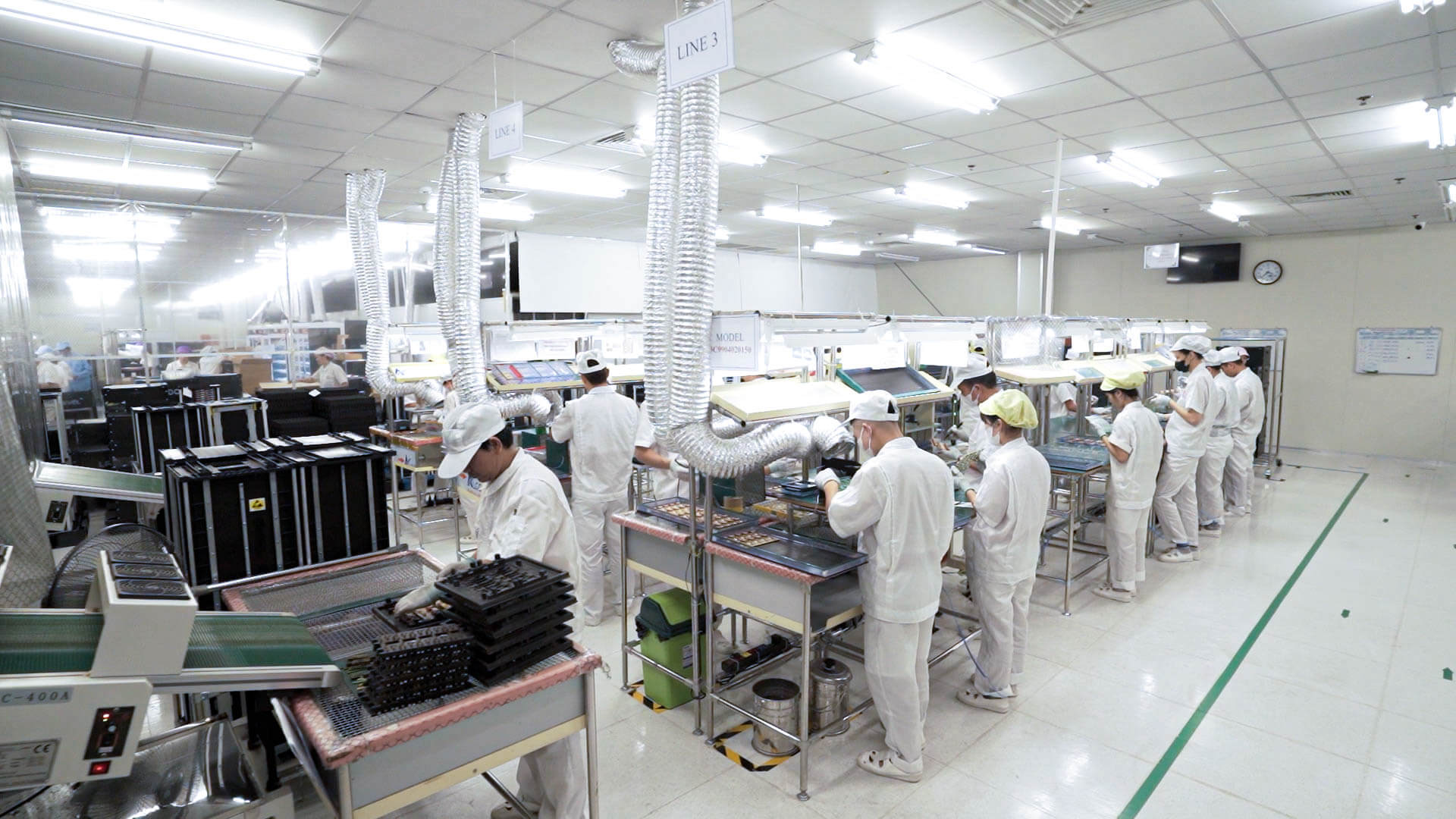
Understanding where NPI programs fail is as important as understanding the process itself. The same failure modes appear repeatedly across industries and product types.
Failure Point 1 — Skipping or Rushing DFM
The pattern: Launch date pressure leads product teams to push directly to prototype build without a thorough DFM review. The first build reveals assembly problems. The second build fixes some of them. By the third build, the program is 6–8 weeks behind schedule and the DFM issues that could have been caught in a 2-day review are now costing weeks of delay.
The fix: Treat DFM review as a non-negotiable gate, not an optional service. A qualified EMS partner should provide a written DFM report before any physical build begins.
Failure Point 2 — BOM Not Manufacturing-Ready
The pattern: Design engineers create BOMs optimized for function and cost — not for manufacturing. Common problems: components specified by value only (no manufacturer part number), single-source critical components, parts available only in cut-tape (not reel), EOL components that will be discontinued before MP ramp.
The fix: BOM scrubbing by the EMS partner’s procurement team at the DFM stage — not at the PVT stage when shortages become schedule-critical. See PCBA contract manufacturing best practices for BOM preparation requirements.
Failure Point 3 — Test Strategy Defined Too Late
The pattern: ICT fixture development is treated as a post-DVT activity. In reality, fixture design, fabrication, and debug takes 4–8 weeks. Starting at PVT stage means test infrastructure isn’t ready when the pilot run completes — delaying MP by months.
The fix: ICT coverage specification and fixture design must begin at DVT stage. FCT jig development should begin in parallel with DVT build. PCBA testing strategy should be defined before process parameters are locked.
Failure Point 4 — EMS Partner Without Dedicated NPI Engineering
The pattern: Many EMS providers treat NPI as a “small production run” — assigning production operators rather than engineers, providing no formal DFM report, setting no go/no-go criteria, and tracking no yield data by phase. The result is a program that reaches MP without a stable process baseline.
The warning signs:
- No DFM report offered as part of NPI service
- No dedicated NPI engineer assigned to the program
- No formal phase gates with defined exit criteria
- No yield tracking by process step during pilot builds
- Process parameters not documented before MP handover
Failure Point 5 — Supply Chain Not Qualified in Parallel
The pattern: Component qualification runs sequentially after design validation — meaning long-lead components (custom magnetics, specific power ICs, RF modules) aren’t ordered until DVT is complete. At MP ramp, the production line is ready but the warehouse is empty.
The fix: Identify long-lead components at DFM stage. Place long-lead orders at DVT stage — before PVT confirms the design. The cost of canceling an order is far lower than the cost of a delayed MP ramp.
For OEMs considering offshore PCB assembly, understanding offshore manufacturing risks — including supply chain qualification gaps — is essential before selecting an NPI partner.
Industry 4.0 in NPI: How Digital Tools Accelerate Time-to-Market
The NPI process has been transformed by digital manufacturing tools. EMS providers operating with Industry 4.0 infrastructure can compress NPI timelines significantly — not by skipping phases, but by accelerating the feedback loops within each phase.
MES-Driven NPI Process Control
A Manufacturing Execution System (MES) integrated from the first prototype build — not just from MP — changes the economics of NPI fundamentally.
In a traditional NPI environment, yield data from a prototype build is collected manually, compiled into a spreadsheet, and analyzed days after the build. In an MES-integrated environment:
- Every placement event, inspection result, and test outcome is captured in real time
- Yield by process step is visible on a dashboard during the build
- Root cause analysis begins while the build is still running — not after it completes
- Process parameter adjustments are made and validated within the same build session
Result: DVT→PVT cycle time reduced by 30–50% in programs where MES data is used actively during NPI.
3D AOI and SPI in NPI Validation
3D SPI (Solder Paste Inspection) at NPI stage validates stencil design before the first reflow cycle. If paste volume is outside specification on specific apertures, the stencil can be corrected before any components are placed — saving an entire build cycle.
3D AOI post-reflow identifies placement and soldering issues with precise coordinate and measurement data — not just pass/fail flags. During NPI, this data is used to optimize placement offsets, reflow profiles, and stencil apertures in real time.
The data generated by 3D SPI and 3D AOI during NPI builds feeds directly into the process parameter documentation for MP — creating a validated, data-backed process baseline rather than one based on engineering judgment alone. See SMT assembly line equipment for the inspection infrastructure that makes this possible.
Automated Test Development
Modern ICT and FCT platforms allow test programs to be developed and simulated digitally before fixture hardware is built. This parallel-path approach — digital test development running alongside DVT build — reduces test fixture development time by 30–40% and eliminates the most common source of NPI schedule delay.
Digital Process Documentation
Industry 4.0 NPI generates process documentation as a byproduct of production — not as a separate documentation effort after the fact:
- Reflow profiles are exported directly from the oven control system
- Placement offsets are extracted from the mounter’s calibration data
- AOI programs become the visual inspection standard for MP
- ICT test programs become the production test specification
Result: MP handover documentation is complete, accurate, and validated by actual production data — not assembled from engineering notes and memory.
External reference: Critical Manufacturing: Bringing Industry 4.0 into the Electronics NPI Process
NPI Checklist: What to Demand From Your EMS Partner
Before awarding an NPI program to a contract manufacturer, use this checklist as a minimum qualification filter. An EMS partner who cannot confirm these capabilities should not be managing your product’s path to production.
NPI Capability Evaluation Checklist
Design Support
- Formal written DFM report provided before first build — not verbal feedback
- DFT (Design for Testability) review included in NPI scope
- BOM scrubbing with lead time, EOL flags, and approved alternate recommendations
- Gerber and schematic review by a qualified process engineer (not a sales engineer)
Prototype & Build Capability
- Dedicated NPI engineering resource assigned — not shared with production floor management
- Small-batch capability (5–50 units) without minimum order quantity penalty
- Build issues log maintained and shared with OEM after each build
- Engineering documentation of all component substitutions and process deviations
Process Development
- Process parameters defined, documented, and validated at DVT stage
- Stencil design support included — aperture optimization for the specific BOM
- Reflow profile development with thermal profiling data provided
- Wave solder / selective solder parameter documentation for through-hole components
Test Infrastructure
- ICT fixture design and build capability — in-house or qualified partner with defined lead time
- FCT jig development support included in NPI scope
- Test coverage report provided — percentage of nets covered by ICT
- Test program development timeline agreed at project kickoff, not after DVT
Pilot Run & Yield Management
- Formal PVT stage with go/no-go criteria defined and agreed before pilot build
- First-pass yield tracked and reported by process step — not just overall yield
- SPC data (Cpk) collected for critical process parameters during pilot
- Written yield improvement plan provided if PVT target is not met at first attempt
Ramp to Mass Production
- Control Plan and PFMEA developed during NPI — not after MP start
- Operator work instructions with visual aids completed before MP handover
- Full traceability active from pilot run — not introduced at MP stage
- Supply chain fully qualified and safety stock established before MP start date
For a broader supplier evaluation framework, see electronics supplier due diligence and electronics factory audit checklist. Understanding IPC standards and ISO standards for manufacturing will also help you evaluate whether an EMS partner’s quality system is genuinely capable of supporting NPI for regulated products.
NPI at SHDC: Engineering-Led, Data-Driven, Production-Ready
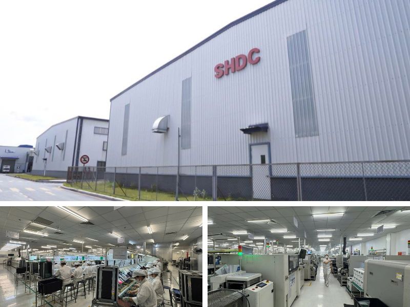
SHDC Electronics is a full-service EMS provider located in the Vietnam Singapore Industrial Park — Hai Duong, 40km from Hanoi and 55km from Haiphong Port. With a 2,600 m² facility, 150 employees, and an integrated Engineering Department comprising both Product Technical and Technical Factory teams, SHDC operates NPI as a distinct engineering discipline — not as a small-batch production service.
Engineering Infrastructure for NPI
Yamaha Smart Factory Integration SHDC’s NPI process is built on Yamaha’s production management ecosystem: S-Tool PC and P-Tool PC for process simulation and program development before first build; YSUP / iProDB for production data management; and YSI-OS for AOI program management. This means process parameters developed during NPI are directly transferable to MP — no re-programming, no re-calibration, no yield regression at ramp.
3D Inspection from Prototype Stage The Yamaha YSI-SP 3D SPI and Yamaha YSI-V 3D AOI systems are active from the first prototype build — not introduced at MP. Solder paste volume data from the first EVT build informs stencil optimization before DVT. AOI data from DVT builds defines the inspection program for PVT and MP.
Precision Placement Capability
- Yamaha YSM20R: ±0.03mm placement accuracy, 95,000 CPH — handles 0402 to 32×32mm components
- Yamaha YSM10: ±0.035mm placement accuracy, 46,000 CPH — handles 03015 to 55×100mm components
- Yamaha YCP10: Screen printer with 1–200mm/sec squeegee speed, 0.4–3.0mm board thickness range
The same equipment used for NPI builds is the production equipment — ensuring that yield data from prototype and pilot builds is directly predictive of MP performance.
ICT and Functional Testing The Kyoritsu ICT F-2000 Plus provides parametric in-circuit test capability. Dedicated FCT stations, aging test equipment, high-voltage test, and AV test infrastructure support comprehensive functional validation from prototype through MP. See in-circuit testing for detailed ICT capability.
Digital Management System SHDC operates an integrated ERP / PLM / SCM / MES / QMS digital infrastructure. The AIT Tracer system provides board-level traceability from the first pilot build. According to SHDC’s production management data, this integration reduces decision-making time by 30% and reduces defective inventory by 30% — outcomes that are particularly valuable during the high-iteration NPI phase.
Proven NPI Track Record
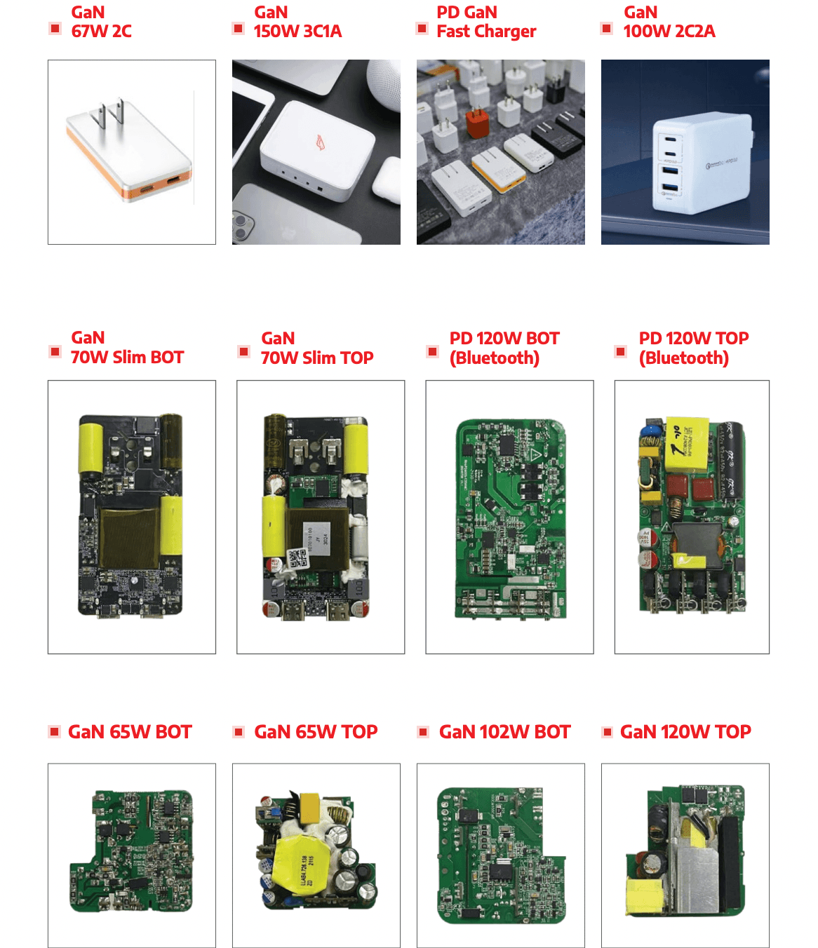
SHDC’s NPI capability has been validated across technically demanding programs:
GaN Power Electronics SHDC has successfully executed NPI for a full range of GaN fast chargers — 65W, 67W, 70W Slim, 100W 2C2A, 102W, 120W (including Bluetooth-enabled), and 150W 3C1A configurations. GaN power electronics represent one of the most demanding NPI challenges in consumer electronics: high-density layouts, tight thermal constraints, and stringent electrical safety requirements. See GaN charger manufacturing in Vietnam and power electronics manufacturing in Vietnam.
Automotive PCBA — Thaco NPI for Thaco automotive PCBA was conducted under PPAP-level documentation requirements — the most rigorous NPI documentation standard in manufacturing. Full Control Plan, PFMEA, and component traceability documentation were produced as part of the NPI deliverable. See automotive PCBA Vietnam.
Industrial and Commercial Electronics NPI programs for PECO industrial electronics, Karofi/Tecomen water purifier control boards, and computer peripherals have demonstrated SHDC’s ability to manage NPI across diverse product types and complexity levels. See industrial electronics manufacturing in Vietnam.
Medical Device Electronics For OEMs requiring ISO 13485-aligned NPI processes — including full component traceability from prototype stage, documented process validation, and DHR-compatible build records — SHDC’s quality infrastructure supports medical device NPI requirements. See medical device electronics manufacturing Vietnam.
Phase 2 Expansion — March 2027
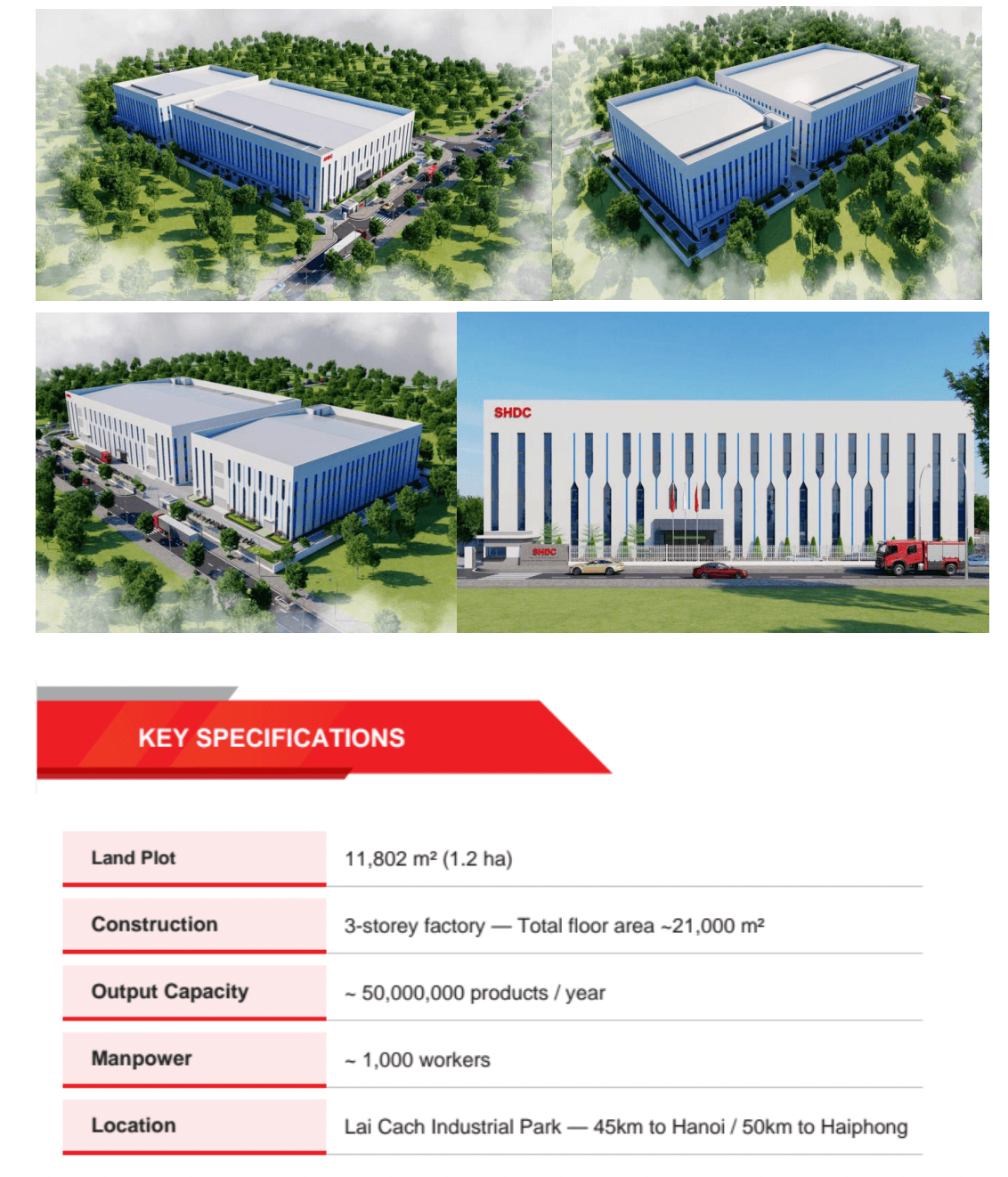
SHDC’s new facility at Lai Cach Industrial Park will add 10 SMT lines, 8 DIP lines, 10 assembly lines, and full inline ICT/FCT/AOI 3D capability — scaling NPI capacity alongside production capacity to support 50M units/year. This means NPI programs started today will have a clear, validated path to high-volume production within the same manufacturing ecosystem.
For OEMs evaluating Vietnam as a manufacturing base, see why Vietnam is the top choice for electronics manufacturing in 2026 and 10 reasons to choose contract electronics manufacturing in Vietnam.
Frequently Asked Questions
What is NPI in electronics manufacturing?
NPI (New Product Introduction) in electronics manufacturing is the structured process of taking a new or redesigned electronic product from its first physical prototype through engineering validation, design validation, and production validation — to a stable, high-yield mass production state. It encompasses DFM review, prototype builds, process development, test fixture creation, pilot runs, and production ramp.
What are the stages of the NPI process in electronics?
The standard NPI process in electronics manufacturing includes five phases: (1) Design Review and DFM Analysis, (2) EVT (Engineering Validation Test) prototype build, (3) DVT (Design Validation Test) with process development, (4) PVT (Production Validation Test) pilot run, and (5) Mass Production ramp. Each phase has defined exit criteria before the next phase begins.
What is the difference between EVT, DVT, and PVT?
EVT (Engineering Validation Test) verifies that the design works as intended — typically 5–20 units with some manual assembly. DVT (Design Validation Test) verifies that the design meets all specifications using production-intent processes — typically 20–50 units. PVT (Production Validation Test) verifies that the production process is stable and repeatable at volume — typically 100–500 units on the actual production line.
How long does NPI typically take for a new PCB product?
NPI timeline depends on product complexity. A straightforward consumer electronics PCB might complete NPI in 8–12 weeks. An industrial or medical device with complex test requirements typically requires 16–24 weeks. The most common cause of NPI timeline extension is test fixture development starting too late and DFM issues discovered at pilot stage rather than design review.
What is DFM and why is it important in NPI?
DFM (Design for Manufacturability) is the analysis of a PCB design against the capabilities and constraints of the production process. It identifies features that will cause assembly problems, yield losses, or test failures before any physical build begins. A thorough DFM review at the start of NPI is the single highest-leverage activity in the entire process — catching issues that would cost 10–100x more to fix at pilot or production stage.
What should I look for in an EMS partner for NPI?
Key indicators of genuine NPI capability: dedicated NPI engineering resource (not production staff), formal written DFM report before first build, defined phase gates with go/no-go criteria, yield tracking by process step during pilot builds, test fixture development starting at DVT stage, and Control Plan/PFMEA delivered as part of MP handover.
Can an EMS partner in Vietnam support full NPI services for U.S. OEMs?
Yes — Vietnam’s leading EMS providers offer full NPI services including DFM review, prototype builds, process development, test fixture creation, and pilot runs. SHDC Electronics in Hai Duong operates Yamaha smart factory infrastructure with integrated MES, 3D AOI, 3D SPI, and ICT/FCT capability — supporting NPI for medical, automotive, industrial, and consumer electronics from prototype through mass production.
Conclusion: NPI Is Where Products Succeed or Fail
The engineering quality of a product’s path from prototype to production determines its commercial viability as much as the design itself. A well-executed NPI process delivers a production program that runs at target yield, ships on schedule, and generates the margins the business model requires. A poorly executed NPI delivers a production program that requires constant engineering intervention, generates chronic quality escapes, and erodes customer confidence.
The regulatory trajectory for electronics manufacturing — particularly in medical, automotive, and industrial segments — is making structured NPI not just a competitive advantage but a compliance requirement. Process validation documentation, traceability from pilot stage, and PFMEA-backed Control Plans are increasingly demanded by OEM customers as conditions of supply.
The right EMS partner for NPI doesn’t just build prototypes — they engineer the path to scalable, documented, auditable production.
