Tiếng Việt
 日本語
日本語
In electronics manufacturing, a product must be both manufacturable and testable. DFM helps OEMs design products that can be built efficiently, while DFT helps ensure those products can be tested reliably during production. For PCBA projects, both DFT and DFM should be reviewed before pilot run and mass production. A board may be easy to assemble but difficult to test. Another board may include enough test points but still create assembly defects because of poor layout, solderability, or panelization. OEMs need both to reduce production risks and improve long-term quality.
What Are DFT and DFM?

DFT and DFM are two important design review methods used in electronics manufacturing. They are often discussed together because both affect production quality, yield, lead time, and cost.
What Is DFM?
DFM stands for Design for Manufacturing. It focuses on whether a PCB or electronic product can be manufactured efficiently, consistently, and cost-effectively.
In PCBA production, DFM usually covers PCB layout, component placement, pad design, panelization, solderability, SMT compatibility, DIP or through-hole assembly, BOM manufacturability, assembly process, and packaging flow.
A strong Design for Manufacturing guide for electronics OEMs helps engineering teams detect manufacturability risks before they become production defects or engineering changes.
Common DFM questions include:
- Can the PCB be fabricated and assembled efficiently?
- Are components spaced correctly for SMT assembly?
- Are pads designed for reliable soldering?
- Is the panelization method suitable for production?
- Is the BOM complete and available for sourcing?
- Are SMT and DIP processes clearly planned?
- Can the final assembly and packaging process run consistently?
DFM answers one core question: can we build this product efficiently at scale?
What Is DFT?
DFT stands for Design for Testability. It focuses on whether a PCB or electronic product can be inspected, tested, diagnosed, and validated efficiently during production.
In PCBA manufacturing, DFT covers PCB test points, ICT access, FCT procedure, AOI visibility, firmware programming, debug access, test fixture planning, pass/fail criteria, and production test records.
A strong Design for Testability guide for electronics OEMs helps OEMs confirm that every production unit can be tested reliably before shipment.
Common DFT questions include:
- Are critical nets accessible for testing?
- Are test pads large enough for probes?
- Is ICT required for this product?
- Is the FCT procedure clearly defined?
- Can AOI inspect critical solder joints?
- Are firmware programming steps planned?
- Are pass/fail criteria measurable?
- Can test data be recorded and traced?
DFT answers another core question: can we verify this product reliably at scale?
DFT vs DFM: Key Differences
DFT and DFM are closely connected, but they are not the same. The difference is simple: DFM focuses on building the product, while DFT focuses on testing the product.
| Area | DFM | DFT |
|---|---|---|
| Full Name | Design for Manufacturing | Design for Testability |
| Main Goal | Make the product easier to manufacture | Make the product easier to test |
| Primary Focus | Assembly, soldering, process flow, BOM, manufacturability | Test points, ICT, FCT, AOI, diagnostics, test coverage |
| Main Risk Reduced | Assembly defects, rework, low yield, production delay | Missed defects, long test time, poor fault detection |
| Typical Review Stage | Before PCB fabrication, pilot run, and mass production | During PCB design, before pilot run, before test fixture design |
| PCBA Example | Adjust component spacing for SMT | Add test points for ICT |
| Outcome | More stable production process | More reliable quality verification |
DFM asks: “Can we build this efficiently?”
DFT asks: “Can we test this reliably?”
Both questions must be answered before mass production. If one side is ignored, OEMs may still face quality, cost, or delivery problems.
Why DFT and DFM Matter Together in Electronics Manufacturing

Manufacturing Without Testability Creates Quality Risk
A board can be easy to assemble but difficult to test. For example, the PCB layout may be suitable for SMT production, but if test points are missing or blocked by tall components, the EMS partner may struggle to perform ICT or failure analysis.
This can lead to:
- Limited test coverage
- More manual troubleshooting
- Longer test cycle time
- Missed electrical defects
- Unclear failure analysis
- Inconsistent outgoing quality
A product that cannot be tested properly creates risk even if the assembly process is stable.
Testability Without Manufacturability Creates Production Risk
The opposite is also true. A board may include test points and a clear FCT plan, but if component spacing, pad design, panelization, or solderability is poor, the project can still suffer from defects and rework.
Common DFM-related production risks include:
- Components too close to board edges
- Unbalanced pads causing tombstoning
- Poor solder paste printing
- Difficult DIP insertion
- Incomplete BOM data
- Poor panelization
- Unclear assembly drawings
A product that is testable but difficult to build will still cause production delays and higher manufacturing costs.
DFT and DFM Improve Production Readiness
Production readiness requires both stable assembly and reliable testing. OEMs should not wait until mass production to discover that a product is hard to build or difficult to test.
A structured Production Readiness Checklist should include both DFM and DFT review. Before pilot production, the OEM and EMS partner should confirm that the design, BOM, process flow, test methods, fixtures, and quality requirements are aligned.
How DFM Works in PCBA Manufacturing
DFM begins with the product design but must be reviewed from the perspective of real manufacturing conditions. In PCBA manufacturing, DFM usually includes PCB layout, component selection, soldering process, assembly flow, and packaging.
PCB Layout and Panelization
PCB layout affects manufacturability from the beginning. A layout that works electrically may still be difficult to assemble or inspect.
OEMs should review:
- Board dimensions
- Panelization method
- Fiducial placement
- Tooling holes
- Board edge clearance
- Depanelization risk
- Component-to-edge spacing
- Mechanical fit with enclosure or fixtures
Poor panelization can slow production, increase handling risk, and create quality issues during depanelization. That is why PCB layout should be reviewed before fabrication files are released.
Component Placement and Solderability
Component placement affects pick-and-place efficiency, solder paste printing, reflow soldering, inspection, and rework.
A DFM review should check whether:
- SMT components have enough spacing
- Fine-pitch components are placed properly
- Pads are designed for solderability
- Thermal balance is considered
- Polarity markings are clear
- Tall components do not block assembly or inspection
- Large thermal pads are designed to reduce voiding
Good component placement supports a more stable SMT assembly process and helps reduce soldering defects.
BOM and Component Selection
The BOM is a key part of DFM. If the BOM is incomplete or includes risky components, the project can face quotation delays, sourcing issues, or production interruptions.
OEMs should review:
- Manufacturer part numbers
- Package sizes
- Reference designators
- Approved alternatives
- Lifecycle status
- Long-lead parts
- MOQ and supplier risk
- Special handling requirements
A complete and accurate BOM also helps the EMS partner prepare a more reliable quote, sourcing plan, and production schedule.
DIP and Through-Hole Assembly
Many PCBAs include both SMT and through-hole components. Connectors, transformers, switches, large capacitors, and mechanical parts may require DIP or through-hole assembly.
A DFM review should check:
- Hole size
- Lead length
- Connector stability
- Component insertion method
- Wave soldering compatibility
- Manual soldering risks
- Mechanical strength
- Inspection access
Understanding SMT vs through-hole assembly helps OEMs choose the right process for each component and avoid unnecessary assembly risk.
How DFT Works in PCBA Manufacturing
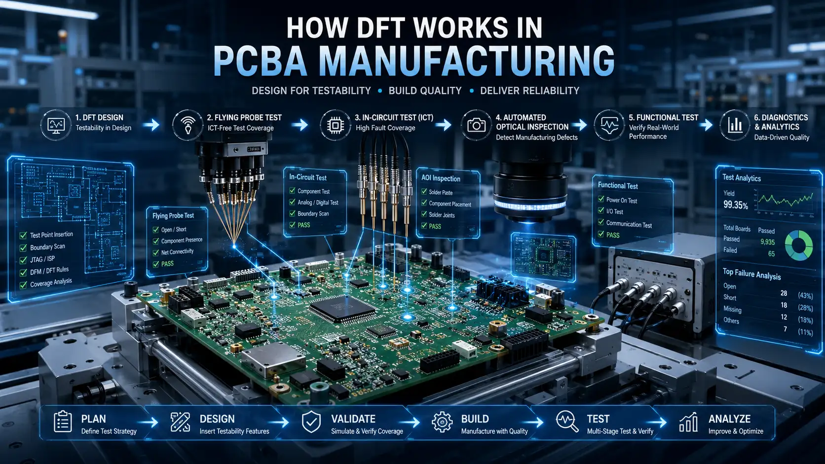
DFT focuses on making the product easier to inspect, test, diagnose, and validate. It should be considered during PCB design, not after the board is already released.
Test Point Design
Test points are one of the most important parts of DFT. They allow probes and fixtures to access electrical nets during ICT, debugging, programming, or functional validation.
OEMs should review:
- Are critical nets accessible?
- Are power and ground test points included?
- Are test pads large enough for probes?
- Is there enough spacing between test points?
- Are test points away from tall components?
- Are test points placed on one side where possible?
- Are high-speed or sensitive signals handled carefully?
- Is the test point map documented?
Poor test point design can reduce test coverage and make troubleshooting more difficult.
ICT Access
In-circuit testing helps detect opens, shorts, component-level issues, and some soldering defects. However, ICT requires physical access to electrical nodes through test pads or probe points.
For ICT readiness, OEMs should confirm:
- Probe access
- Test pad size
- Test point spacing
- Bed-of-nails fixture compatibility
- Power and ground coverage
- Critical net coverage
- Components that may be difficult to test
- Fixture alignment and mechanical access
ICT is not required for every product, but for complex or higher-volume PCBAs, it can be an important quality control method.
FCT Planning
Functional circuit testing, or FCT, verifies whether the PCBA performs its intended functions. It may test power behavior, communication, sensors, buttons, motors, relays, LEDs, firmware, or external loads.
A good FCT plan should define:
- Functional test procedure
- Power input conditions
- Output signals
- Communication protocols
- Required firmware version
- Pass/fail limits
- Test fixture requirements
- Test data recording
- Retest and failure handling process
FCT should be planned before pilot production because fixtures, test software, and operator instructions may take time to prepare.
AOI and Visual Inspection
Automated optical inspection helps detect placement, polarity, missing components, and visible soldering defects. For AOI to work effectively, the PCB layout must support visual access.
OEMs should check:
- Are component markings visible?
- Are polarity indicators clear?
- Are solder joints visible?
- Are similar components easy to distinguish?
- Are tall components blocking inspection?
- Are critical components highlighted in drawings?
DFT is not only about electrical testing. It also includes inspection access and quality verification.
DFT and DFM Checklist for Electronics OEMs
A practical checklist helps OEMs review manufacturability and testability before production files are finalized.
DFM Checklist
Use this DFM checklist before PCB fabrication, prototype build, pilot run, or mass production:
- Are PCB dimensions suitable for production equipment?
- Is the panelization method defined?
- Are fiducials included?
- Are components spaced correctly?
- Are components too close to board edges?
- Are pads designed for solderability?
- Are polarized components clearly marked?
- Is the BOM complete and accurate?
- Are long-lead components identified?
- Are approved alternatives listed?
- Are SMT and DIP processes clearly planned?
- Are assembly drawings complete?
For a more detailed practical list, OEMs can use a DFM checklist for PCBA manufacturing.
DFT Checklist
Use this DFT checklist before test fixture design, pilot run, or mass production:
- Are test points included for critical nets?
- Are power and ground points accessible?
- Are test pads large enough for probes?
- Are test points away from tall components?
- Is ICT required for this product?
- Is the expected test coverage defined?
- Is the FCT procedure written?
- Are pass/fail criteria clear?
- Is firmware programming planned?
- Can AOI inspect critical solder joints?
- Are retest and failure handling rules defined?
- Are test data and traceability requirements documented?
Shared DFT and DFM Checklist
Some items affect both manufacturability and testability:
- Are design files complete?
- Is the BOM frozen before pilot run?
- Are manufacturing and testing risks reviewed together?
- Are fixture requirements defined?
- Are quality standards confirmed?
- Are pilot run goals clear?
- Are engineering change rules agreed?
- Is the EMS partner involved before mass production?
DFT and DFM work best when they are reviewed together instead of separately.
Common Mistakes When OEMs Treat DFT and DFM Separately
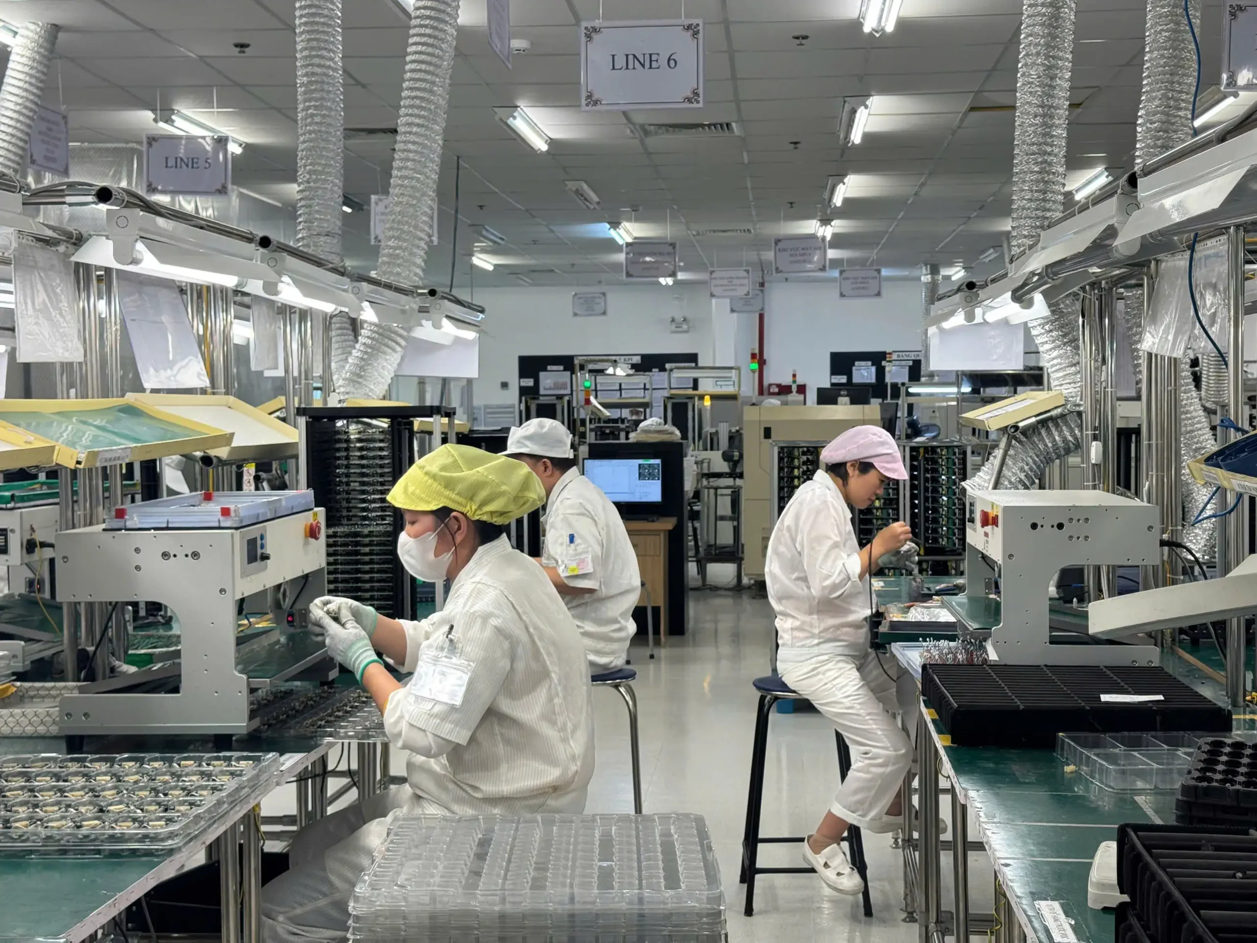
Adding Test Points After PCB Layout Is Frozen
If test points are added too late, the PCB may need a layout revision. This can delay pilot production and increase engineering workload.
Designing for Prototype Instead of Production
A hand-built prototype may work, but that does not mean the product is ready for automated assembly and production testing. Prototype success should be followed by DFM and DFT review.
Ignoring Test Fixture Requirements
ICT and FCT fixtures require mechanical access, test pads, connectors, cable routing, and operating procedures. If fixture requirements are ignored early, production testing can become slow or inconsistent.
Focusing Only on Unit Cost
A low unit cost does not always mean lower total cost. Rework, failed testing, long test time, engineering changes, low yield, and manual inspection can all increase real production cost.
OEMs should review PCB assembly cost together with manufacturability and testability factors.
Not Aligning Engineering, Quality, and EMS Teams
DFT and DFM require collaboration. Design engineers, manufacturing engineers, quality teams, and EMS partners should review the product together before pilot run.
DFT and DFM During the Product Development Process
DFT and DFM should appear throughout the product development process, not only at the end.
During PCB Design
DFM focus:
- Layout
- Spacing
- Pad design
- Panelization
- Component selection
DFT focus:
- Test points
- Programming access
- ICT access
- FCT access
- Debug interface
Before Prototype Build
DFM focus:
- Fabrication files
- BOM accuracy
- Assembly requirements
- Initial process feasibility
DFT focus:
- Initial test plan
- Basic functional test
- Debug access
- Firmware programming method
Before Pilot Run
DFM focus:
- Process flow
- SMT and DIP setup
- Assembly fixtures
- Work instructions
- Material readiness
DFT focus:
- ICT or FCT fixture
- Test coverage
- Pass/fail criteria
- Test cycle time
- Failure handling
Before Mass Production
DFM focus:
- Yield stability
- Production process control
- Material availability
- Packaging readiness
DFT focus:
- Test records
- Traceability
- Retest rules
- Failure analysis
- Outgoing quality control
When DFT and DFM are reviewed at each stage, OEMs can reduce late changes and improve production confidence.
How DFT and DFM Affect Cost, Quality, and Lead Time
Cost Impact
Good DFM reduces assembly defects, rework, scrap, and inefficient production steps. Good DFT reduces troubleshooting time, missed defects, retest confusion, and manual inspection workload.
Together, DFT and DFM help reduce hidden manufacturing costs. These costs often appear after quotation, during pilot run, or when production volume increases.
Quality Impact
DFM improves build consistency. It helps the PCBA move through fabrication, SMT assembly, through-hole assembly, inspection, and packaging with fewer defects.
DFT improves verification consistency. It helps the EMS partner test each unit more reliably and detect problems before shipment.
Together, they support stronger PCBA quality control.
Lead Time Impact
Late DFM and DFT issues can delay production. Examples include PCB redesign, BOM replacement, fixture redesign, unclear FCT procedure, and repeated pilot run failures.
A clear process for Engineering Change Orders can help control changes when they are necessary, but the best approach is to prevent avoidable changes through early review.
What OEMs Should Prepare for a DFT and DFM Review
To get useful feedback from an EMS partner, OEMs should prepare a complete technical package.
Recommended files and information include:
- Product specification
- Gerber files
- Schematic
- BOM
- Pick-and-place file
- Assembly drawing
- PCB stack-up requirements
- Target production volume
- Quality requirements
- ICT or FCT requirements
- Firmware instructions
- Mechanical files
- Packaging requirements
- Expected pilot run schedule
- Customer-specific requirements, if applicable
The more complete the files are, the more accurate the DFT and DFM review will be. Incomplete files may still allow a preliminary review, but they can limit the quality of feedback.
Questions OEMs Should Ask Their EMS Partner
Before starting pilot production, OEMs should ask their EMS partner:
- Do you see any PCB layout risks?
- Is the design suitable for SMT and DIP assembly?
- Are there any BOM sourcing risks?
- Is the panelization design suitable for production?
- Are test points sufficient for ICT?
- Is FCT required for this product?
- What test coverage can be achieved?
- Are any components difficult to inspect with AOI?
- What fixture requirements should we plan?
- What should be validated during pilot production?
- What changes would improve yield or test efficiency?
These questions are also useful during EMS provider selection, especially for OEMs comparing manufacturing partners in Asia.
How SHDC Supports DFT and DFM for Electronics OEMs
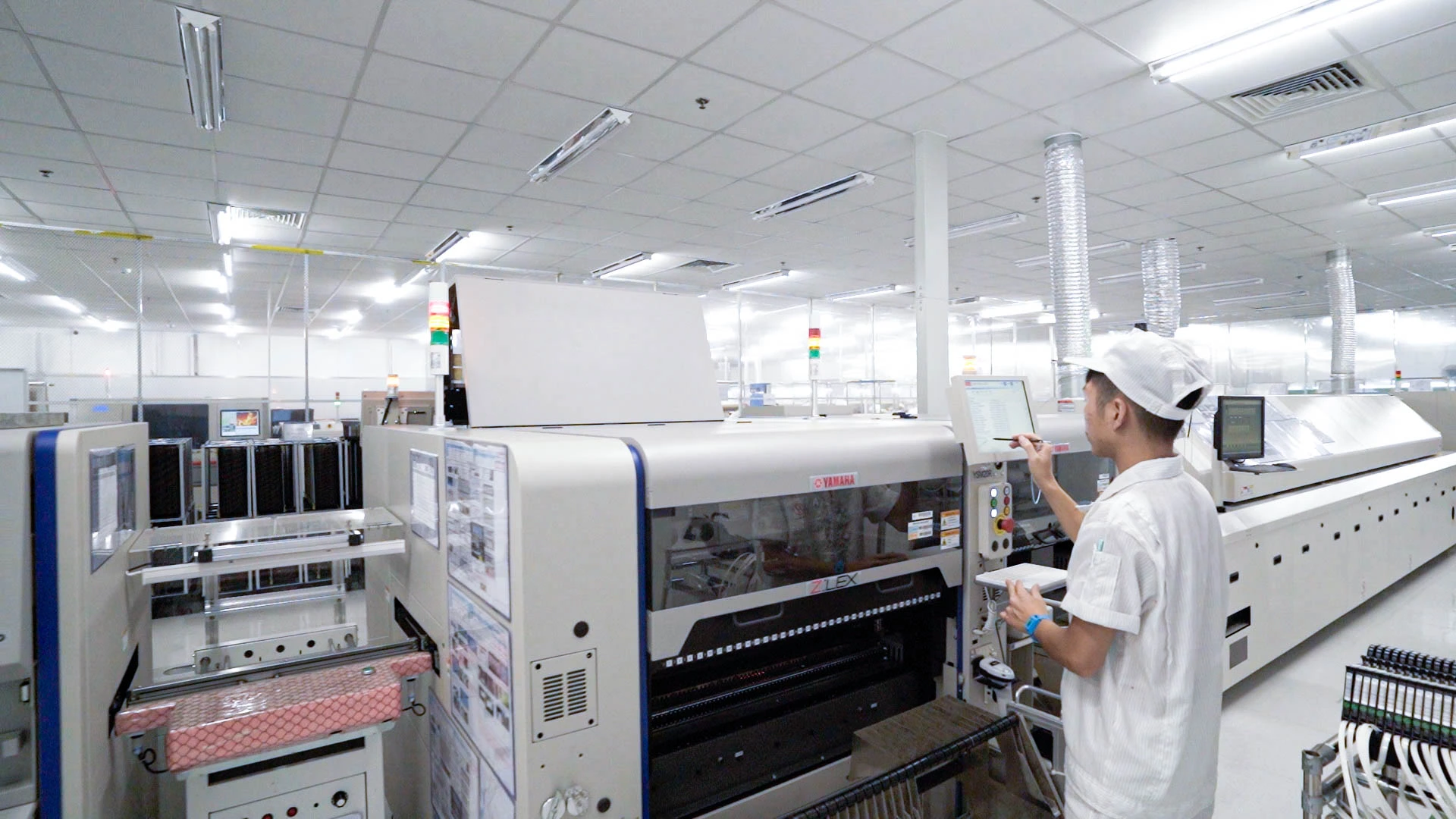
SHDC supports electronics manufacturing services for OEM customers, including SMT, DIP, assembly, testing, and packaging. This makes SHDC relevant for both manufacturability and testability review.
From a DFM perspective, SHDC can support PCBA projects through SMT processing, DIP assembly, component insertion, soldering, assembly, and packaging. These production steps are important when reviewing PCB layout, component placement, BOM readiness, solderability, and production flow.
From a DFT perspective, SHDC’s process includes inspection and testing stages such as AOI, ICT, FCT, visual inspection, OQC, and final quality control. Testing-related capabilities such as AOI 3D, ICT, functional testing, high-voltage testing, A/V testing, and aging testing can help OEMs review testability before pilot run and mass production.
SHDC also supports PCBA applications such as chargers, power-related electronics, water purifier boards, computer mouse boards, petrol-related electronics, and automotive-related PCBA. For U.S. OEMs evaluating electronics manufacturing in Vietnam, SHDC can support projects from design review to PCBA production, testing, final assembly, and packaging.
OEMs that need integrated manufacturing support can also consider full-service EMS in Vietnam for a broader production scope.
>>>Read more: Industrial Electronics Manufacturing in Vietnam: Capabilities, Certifications & EMS Services at SHDC
Final Thoughts
DFT and DFM are different but closely connected. DFM helps OEMs build PCBAs efficiently, while DFT helps verify them reliably. In electronics manufacturing, both should be reviewed before pilot run and mass production.
A product that is easy to build but hard to test creates quality risk. A product that is easy to test but difficult to manufacture creates production risk. The best approach is to review DFT and DFM together with the EMS partner early in the project.
If you are preparing a PCBA project for production, SHDC can help review your DFT and DFM requirements and support manufacturing from SMT and DIP assembly to AOI, ICT, FCT, final inspection, and packaging.
FAQs About DFT and DFM
What does DFT and DFM mean?
DFT stands for Design for Testability, while DFM stands for Design for Manufacturing. DFT focuses on testing, while DFM focuses on manufacturability.
What is the difference between DFT and DFM?
DFM answers whether a product can be manufactured efficiently. DFT answers whether the product can be tested reliably during production.
Why are DFT and DFM important in electronics manufacturing?
They help reduce assembly defects, improve test coverage, lower rework risk, shorten production delays, and support more stable PCBA quality.
Should DFM or DFT come first?
They should be reviewed together during PCB design. DFM affects assembly quality, while DFT affects inspection, testing, and failure detection.
How does DFM affect PCBA quality?
DFM improves PCB layout, component placement, solderability, panelization, BOM readiness, and assembly flow. This helps reduce production defects and rework.
How does DFT affect PCBA testing?
DFT improves test point access, ICT feasibility, FCT planning, AOI visibility, firmware programming, fault detection, and production test consistency.
Can an EMS partner help with both DFT and DFM?
Yes. A capable EMS partner can review manufacturability and testability from a production-floor perspective before pilot run or mass production.