Tiếng Việt
 日本語
日本語
A PCB design is not ready for production simply because the schematic and layout are complete. Before a contract manufacturer can fabricate the bare board, procure components, program placement equipment, assemble the PCBA, and perform testing, the OEM must release a complete and internally consistent set of PCB assembly files.
At minimum, the manufacturing package normally includes fabrication data, a bill of materials, component coordinates, and assembly drawings. More complex products may also require schematics, test specifications, firmware, mechanical files, labeling instructions, and special-process requirements.
Missing information does more than delay production. It can create quotation assumptions, component-placement errors, incorrect product variants, unnecessary engineering questions, and revision-control risks. This guide explains what each PCB assembly file does, what information it should contain, and how OEM teams can review the complete package before sending it to a manufacturer.
What Are PCB Assembly Files?
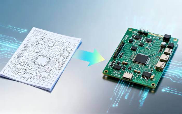
PCB assembly files are the digital documents and datasets used to convert an electronic design into a physically assembled circuit board.
They are not all used for the same purpose. Some files communicate how the bare PCB must be fabricated, while others tell the manufacturer which components to purchase, where to place them, how to orient them, and how to inspect or test the finished assembly.
Modern PCB design software can generate multiple types of manufacturing output, including Gerber, drill, ODB++, IPC-2581, bill of materials, and pick-and-place data. The exact package should be agreed upon with the manufacturer because production systems and preferred file formats may differ.
PCB fabrication files vs. PCB assembly files
PCB fabrication files define the bare circuit board. They normally communicate:
- Copper layers
- Solder mask
- Silkscreen
- Board outline
- Drill locations
- Slots and routed features
- Mechanical information
- Fabrication notes
PCB assembly files define how electronic components and other parts are installed on that board. They commonly communicate:
- Component part numbers
- Quantities
- Reference designators
- X-Y placement coordinates
- Rotation
- Top or bottom side
- Polarity
- Pin 1 orientation
- DNP or DNI status
- Manual assembly instructions
- Testing and programming requirements
For a turnkey project, the manufacturer usually requires both groups. The fabrication package supports bare-board production, while the assembly package supports procurement, SMT programming, through-hole assembly, inspection, testing, and final acceptance.
OEMs preparing a production release can also review this PCBA manufacturer Vietnam RFQ checklist to confirm that commercial and project-level information is provided alongside the technical files.
Minimum files required for PCB assembly
| File | Main purpose | Typical status |
|---|---|---|
| Gerber or intelligent PCB data | Defines the PCB layers and artwork | Required |
| NC drill and route files | Defines holes, slots, and routed features | Required |
| Bill of Materials | Defines the parts to procure and install | Required |
| Pick-and-place file | Provides component coordinates and rotation | Required for automated SMT |
| Assembly drawing | Shows component locations, orientation, and notes | Required |
| Schematic | Supports engineering review and troubleshooting | Strongly recommended |
| Test specification | Defines test methods and pass/fail limits | Project-dependent |
| Firmware package | Defines programming data and verification | Project-dependent |
| Mechanical files | Supports enclosure and final-product integration | Project-dependent |
The manufacturer may request additional documents depending on the product, regulatory requirements, test coverage, supply model, and level of assembly.
Gerber, ODB++ and Drill Files
What Gerber files contain
Gerber is widely used to transfer graphical PCB fabrication data. A conventional release generally contains separate files for individual board layers, such as:
- Top and bottom copper
- Internal copper layers
- Top and bottom solder mask
- Top and bottom silkscreen
- Top and bottom solder paste
- Board outline
- Mechanical or documentation layers
Ucamco’s official Gerber specification defines Gerber as a format for representing PCB fabrication data. Because a single Gerber file generally represents one two-dimensional layer image, the manufacturer must receive the complete and correctly identified layer set.
Before release, the OEM should review the exported dataset in an independent Gerber viewer rather than relying only on the original PCB editor. The check should confirm:
- All expected layers are present
- Copper and solder-mask data align
- Silkscreen does not cover exposed pads
- The board outline is continuous
- Paste layers reflect the intended stencil apertures
- Mechanical layers are clearly identified
- No obsolete or duplicate layers remain in the package
NC drill and route data
Drill files identify holes and other machined features that cannot be communicated only through graphical copper layers. Depending on the board, they may include:
- Plated through-holes
- Non-plated holes
- Via holes
- Blind or buried via information
- Slots
- Cutouts
- Routed contours
- Tool diameters
The release should clearly state the measurement unit, coordinate format, zero suppression, and distinction between plated and non-plated features. When routing information is placed in a mechanical Gerber layer instead of a separate route file, the README or fabrication drawing should explain how the data must be interpreted.
Gerber vs. ODB++ and IPC-2581

Gerber remains common, but intelligent manufacturing-data formats can combine more product information into a structured dataset.
ODB++Design is intended to transfer PCB design information into fabrication, assembly, and test through an integrated data structure. The format can reduce the need to manually reconstruct relationships between separate files, although acceptance still depends on the manufacturer’s CAM and production systems.
IPC-2581 is another intelligent data-exchange format for printed boards and assemblies. IPC describes it as a digital manufacturing-description and transfer methodology, while current PCB tools such as KiCad can export both IPC-2581 and ODB++ datasets.
The OEM should not assume that one format is universally superior. Confirm which format the selected PCB assembly manufacturer prefers, and do not mix independently generated datasets unless their revision and content have been verified.
Common fabrication-file problems
Typical problems include:
- Missing solder-paste layers
- An incorrect or open board outline
- Conflicting dimensions between the drawing and data
- Unidentified mechanical layers
- Drill files generated in different units
- Incorrect plated/non-plated hole classification
- Files exported from different design revisions
- Old fabrication data left in the release ZIP
These problems should be found before quotation or engineering build. A structured DFM checklist for PCBA manufacturing can help the OEM and manufacturer review whether the design and output package are ready for production.
Bill of Materials Requirements for PCB Assembly
The Bill of Materials, or BOM, tells the manufacturer what must be purchased and installed. It is not simply a list of component values. A production-ready BOM must identify parts precisely enough for procurement, incoming inspection, kitting, placement, traceability, and change control.
Altium describes the BOM as the report that lists the components required to build the product and guides procurement of the assembly.
Required BOM columns
A useful PCB assembly BOM normally contains:
| BOM field | Purpose |
|---|---|
| Reference designator | Links each part to its PCB location |
| Quantity | States the number required per assembly |
| Manufacturer | Identifies the original component manufacturer |
| Manufacturer part number | Defines the exact purchasable part |
| Description | Provides a readable technical description |
| Value | Shows electrical value where applicable |
| Package or footprint | Supports cross-checking with PCB data |
| DNP/DNI status | Identifies parts that must not be installed |
| Approved alternatives | Controls permitted substitutions |
| Supply responsibility | Identifies customer-supplied or manufacturer-sourced parts |
| Product variant | Distinguishes configuration-specific parts |
| Notes | Communicates special procurement or assembly conditions |
Descriptions such as “10 kΩ resistor” or “USB connector” are usually insufficient on their own. They do not define tolerance, voltage rating, power rating, package, manufacturer, plating, temperature grade, or other attributes that may affect compatibility.
How to identify DNP and optional components
Components that are not to be populated should be marked consistently as DNP, DNI, or another mutually agreed status.
The OEM should not simply delete them from one file while leaving them active elsewhere. A DNP component can still appear in the design database, but its status must match across:
- BOM
- Pick-and-place file
- Assembly drawing
- Product variant definition
- Test documentation
If a reference designator is marked DNP in the BOM but remains active in the pick-and-place file, the manufacturer must stop and request clarification. If that conflict is missed, an unwanted component could be installed.
Common BOM errors
Frequent BOM problems include:
- Missing manufacturer part numbers
- Duplicate reference designators
- Quantity not matching the RefDes count
- Package information that conflicts with the PCB footprint
- Unclear alternative-part approval
- Obsolete or unavailable components
- Inconsistent DNP status
- Multiple product variants combined without clear rules
- Internal descriptions that cannot be matched to purchasable parts
- Uncontrolled spreadsheet edits after design release
The BOM should be checked against the component-placement data before it is issued. This article does not replace a complete sourcing review; OEMs that need quotation planning should also consult the PCB assembly quote requirements.
Pick-and-Place and Centroid File Requirements
A pick-and-place file provides the coordinate data used to program automated component-placement equipment.
Altium’s assembly documentation states that pick-and-place output records the location, rotation, and board side for each included component. The file can commonly be produced as CSV or text, although individual manufacturers may request a specific column structure.
What a pick-and-place file contains
The file should normally include:
- Reference designator
- X coordinate
- Y coordinate
- Rotation
- Top or bottom side
- Footprint or package
- Component value or part identifier
- Product variant status where applicable
Some manufacturers also request fields such as feeder description, nozzle information, mounting type, component height, or manufacturer part number. These fields may be added by the manufacturer during process engineering rather than supplied directly by the OEM.
Coordinate origin, units, and rotation
Coordinate data is only useful when its conventions are clear.
The release should identify:
- Whether coordinates use millimeters or inches
- The location of the X-Y origin
- Whether the origin is based on the board or production panel
- Positive axis directions
- Rotation convention
- How bottom-side components are represented
- Whether coordinates refer to the component centroid, body center, or another defined point
Rotation is a frequent source of confusion because different ECAD tools, libraries, component models, and placement systems may interpret zero degrees differently. For polarized components, the manufacturer should verify the file against the assembly drawing, silkscreen, footprint, and datasheet during NPI preparation.
Pick-and-place file vs. centroid file
“Pick-and-place file,” “centroid file,” “component-position file,” and “XY file” are often used for the same general category of component-location data.
The names do not guarantee an identical format. One file may include only RefDes, X, Y, rotation, and side, while another may contain additional value, package, and variant information. The manufacturer should confirm the required template before the OEM releases production data.
Pick-and-place verification checklist
Before submission, confirm that:
- Every active RefDes exists in the BOM
- Every SMT component intended for placement is included
- DNP parts are excluded or clearly identified
- Coordinates fall within the correct board or panel outline
- Units are declared
- The coordinate origin is documented
- Top and bottom sides are identified correctly
- Rotation values match the design
- Polarized parts have clear orientation references
- Quantities agree with the BOM
PCB Assembly Drawing Requirements

The assembly drawing communicates information that cannot always be understood safely from raw coordinates alone.
It should provide a readable top and bottom view of the board, identify component locations, and show orientation details for polarized or mechanically sensitive parts. Altium’s PCB assembly documentation guide emphasizes drawings, assembly notes, and cautionary markings as key elements of a successful assembly release.
Information shown on an assembly drawing
A complete drawing may include:
- Board outline
- Component outlines
- Reference designators
- Top and bottom views
- Pin 1 indicators
- Polarity markings
- Diode and LED orientation
- Connector orientation
- Mechanical hardware
- Mounting-hole information
- DNP markings
- Component-height restrictions
- Revision number
- Drawing number
- General assembly notes
Reference designators must remain legible. When the board is too dense to show all identifiers clearly, the OEM can provide enlarged detail views or separate drawings for each side.
Special assembly notes
Special instructions may address:
- Hand-soldered components
- Press-fit connectors
- Parts installed after cleaning
- Components sensitive to wash processes
- Adhesive application
- Thermal-interface materials
- Heat sinks and mechanical fasteners
- Torque requirements
- Cable orientation
- Selective soldering restrictions
- Conformal-coating exclusions
- Masked test points
- Labels and serialization
These instructions should be specific and measurable. A note such as “install carefully” does not define an acceptable process or result.
Top and bottom drawings
For double-sided assemblies, issue clearly labeled top and bottom drawings. Do not assume that a mirrored screenshot is self-explanatory.
The manufacturer must be able to distinguish:
- Viewing direction
- Actual component side
- Pin 1 orientation
- Reference-designator location
- Mechanical datum
- Product variant
Supporting Files for Complex PCBA Projects
Not every assembly requires every document below. However, the more complex the product, the less safe it becomes to rely only on Gerber, BOM, and coordinate data.
Schematic and netlist
The schematic helps engineers understand circuit relationships and expected behavior. It can support:
- Design review
- DFT review
- Test development
- Debugging
- Failure analysis
- Confirmation of component function
- Comparison between intended and measured connectivity
A connectivity netlist can also support electrical comparison or test preparation. The exact requirement should be agreed upon before release.
Test specifications
A test specification should define how the assembly will be evaluated rather than merely stating “perform functional testing.”
Depending on the product, it may include:
- Test stage
- Required equipment
- Fixture information
- Test-point locations
- Input voltage and current
- Expected output
- Measurement tolerances
- Test sequence
- Pass/fail criteria
- Data-recording requirements
- Retest rules
- Sample size
- Handling of failed units
OEM teams designing test coverage can review the role of AOI, ICT, and functional testing in this PCBA testing guide.
Firmware and programming files
When devices require programming, provide:
- Firmware binary or approved programming file
- Firmware version
- Product variant
- Programming tool and interface
- Device configuration
- Fuse or security settings
- Checksum or hash
- Verification method
- Labeling or serialization rule
- Retention requirements for programming records
The firmware version should also appear in the release manifest. Sending a programming file separately by email after the production package has been approved increases the risk of an uncontrolled mismatch.
Mechanical and 3D files
STEP models, enclosure drawings, cable drawings, heat-sink drawings, and final-assembly instructions can help identify interference, orientation, connector access, and dimensional constraints.
These files become especially important when the manufacturer performs box build assembly services in addition to PCBA production.
Special-process specifications
Complex projects may require instructions for:
- Lead-free soldering
- Cleaning
- Conformal coating
- Potting
- Underfill
- Staking
- Adhesive dispensing
- Laser marking
- Label application
- Serialization
- Special packaging
- Moisture-barrier protection
The specification should state the required material, application area, prohibited area, inspection method, and acceptance criteria where applicable.
Revision Control Across PCB Assembly Files
Even technically correct files can produce the wrong assembly when they belong to different revisions.
The following documents should be checked as one controlled release:
- PCB source design
- Gerber or intelligent data package
- Drill files
- BOM
- Pick-and-place file
- Assembly drawing
- Schematic
- Test specification
- Firmware
- Mechanical drawing
- Packaging instructions
Common PCB Assembly File Errors
| Error | Potential impact | Recommended control |
|---|---|---|
| BOM and pick-and-place mismatch | Missing or incorrectly placed components | Compare RefDes automatically |
| Wrong rotation values | Incorrect component orientation | Verify against drawing and datasheet |
| Unclear DNP status | Unwanted parts may be installed | Synchronize BOM, XY file, and drawing |
| Mixed revisions | Product built to the wrong configuration | Release files through one approved package |
| Missing assembly drawing | Special orientation may be unclear | Provide top and bottom drawings |
| Missing test limits | Pass/fail decision becomes subjective | Issue measurable test criteria |
| Units not declared | Coordinate or dimensional errors | State mm or inch explicitly |
| Missing board outline | CAM interpretation may be delayed | Include and identify the profile layer |
| Generic BOM descriptions | Procurement ambiguity | Include manufacturer and MPN |
| Firmware sent separately | Wrong software version may be loaded | Control firmware in the release manifest |
A broader system for managing design documents, changes, approvals, and production records is discussed in SHDC’s guide to PCBA documentation controls.
PCB Assembly File Checklist Before Submission
Use this checklist before issuing the final package:
- Gerber, ODB++, or IPC-2581 data has been generated from the approved design.
- Gerber files have been reviewed in an independent viewer.
- Copper, solder-mask, silkscreen, and paste layers are complete.
- Board-outline data is present and unambiguous.
- Drill and route files are included.
- Plated and non-plated features are identified.
- The BOM includes manufacturer names and part numbers.
- BOM quantities match the reference-designator count.
- DNP components are marked consistently.
- Approved substitutions are defined.
- Pick-and-place data includes X, Y, rotation, side, and units.
- The coordinate origin is documented.
- BOM and pick-and-place reference designators match.
- Assembly drawings show polarity and pin 1.
- Top and bottom assembly views are clearly labeled.
- Schematics are included when required for review or testing.
- Test specifications define measurable pass/fail criteria.
- Firmware includes version and verification information.
- Mechanical and special-process documents are included where applicable.
- Every file is listed in the revision matrix.
- Only approved files are included in the release folder.
- A README explains unusual layers, formats, or instructions.
- The complete package is reviewed before being sent for quotation or production.
How Complete Files Improve PCBA Production
Complete PCB assembly files allow the manufacturer to review the project with fewer assumptions. They support more accurate quotation, clearer component sourcing, faster NPI preparation, consistent machine programming, objective testing, and controlled production changes.
They also allow technical questions to be raised before materials are ordered or boards enter assembly. This is particularly important when an OEM is qualifying a new PCB assembly Vietnam partner or transferring an existing product from another factory.
How SHDC Supports PCB Assembly File Review
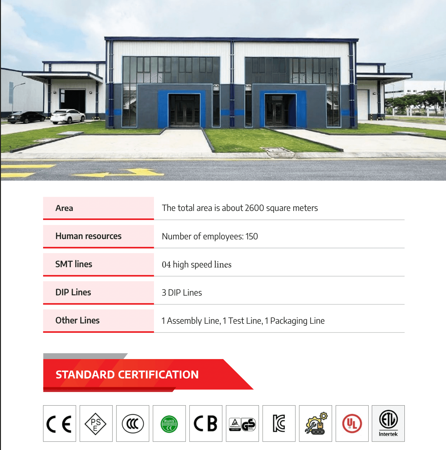
SHDC Electronics provides EMS activities from component soldering and assembly through testing and final packaging. Its company profile lists four high-speed SMT lines, three DIP lines, one assembly line, one test line, and one packaging line at its Vietnam operation.
For an OEM project, the technical release package should be reviewed before procurement and production planning begin. Gerber or intelligent PCB data, BOM, pick-and-place information, drawings, test requirements, and revision records must describe the same approved product configuration.
OEM teams considering production in Vietnam can learn more about SHDC’s broader PCBA Vietnam capabilities and submit a controlled data package for technical review.
Conclusion
Reliable PCB assembly begins with reliable data. A complete package requires more than Gerber files and a parts list. The BOM, pick-and-place file, assembly drawings, schematics, test requirements, firmware, mechanical documents, and revision matrix must all describe the same product.
Before requesting a quotation or approving a pilot build, verify every PCB assembly file, remove obsolete documents, resolve conflicts, and release one controlled package. This preparation reduces avoidable clarification, sourcing, placement, testing, and revision risks throughout the PCBA program.
Frequently Asked Questions
What files are required for PCB assembly?
The minimum package normally includes Gerber or another accepted fabrication-data format, drill files, a BOM, a pick-and-place file, and assembly drawings. Complex products may also require schematics, test specifications, firmware, mechanical files, and special-process instructions.
Are Gerber files enough for PCB assembly?
No. Gerber files primarily communicate PCB layer artwork and fabrication data. The assembler also needs component information, placement coordinates, orientation instructions, and any applicable testing or programming requirements.
What information should a PCB BOM include?
A production BOM should include reference designators, quantity, manufacturer, manufacturer part number, description, value, package, DNP status, approved alternatives, and supply responsibility.
What is the difference between a pick-and-place file and a centroid file?
The terms are often used for the same general type of component-position data. Both normally communicate X-Y coordinates, rotation, board side, and reference designators, but column formats may differ.
Does a PCB assembler need the schematic?
A schematic may not always be required to place components, but it is highly useful for engineering review, test development, troubleshooting, and failure analysis.
How should DNP components be identified?
DNP or DNI status should be consistent across the BOM, pick-and-place file, assembly drawing, and product-variant definition.
Should OEMs use Gerber or ODB++?
Both may be suitable. Gerber uses separate layer files, while ODB++ can transfer more structured product information in one integrated dataset. The OEM should confirm the manufacturer’s preferred format before release.
How can OEMs prevent PCB file revision mismatches?
Use a revision matrix, standardized file names, a controlled release folder, and a formal change process. Send only one approved package and remove superseded files before submission.