
 Tiếng Việt
 日本語
日本語
A bare printed circuit board becomes a functional PCBA only after components are mounted, soldered, inspected and electrically tested. Each stage of the PCB assembly process controls a different manufacturing risk, from incorrect materials and insufficient solder paste to placement errors, soldering defects and functional failures.
At SHDC, the documented production flow combines surface-mount technology, through-hole assembly, automated optical inspection and electrical testing. The process shown in the company profile begins with incoming quality control and material preparation, then continues through solder paste printing, SMT placement, reflow, AOI, DIP insertion, automatic soldering, ICT, FCT, outgoing inspection and packaging.
This article explains how those stages work, what each inspection method can detect and what US OEMs should provide before sending a PCBA project for manufacturing review.
What Is the PCB Assembly Process?
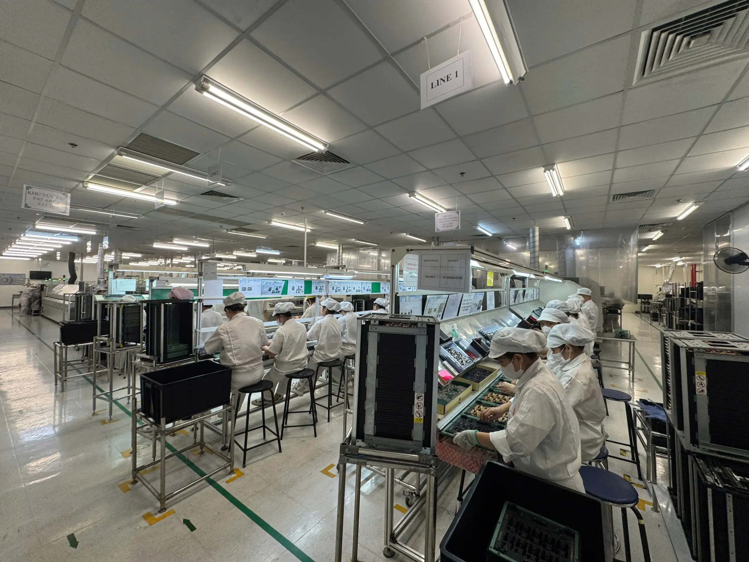
The PCB assembly process is the sequence of operations used to mount and solder electronic components onto a fabricated printed circuit board.
A PCB is the unpopulated board containing copper traces, pads, vias and insulating layers. Once electronic components have been installed and soldered, it becomes a printed circuit board assembly, or PCBA.
PCB fabrication and PCB assembly are therefore two separate manufacturing stages:
- PCB fabrication creates the bare circuit board.
- PCB assembly installs components and produces the functional electronic assembly.
For a broader introduction to the difference between these stages, see SHDC’s guide explaining what PCBA manufacturing.
A typical assembly project may use:
- Surface-mount technology for small, high-density components
- Through-hole assembly for connectors, transformers and larger mechanical parts
- Reflow or wave soldering
- Optical and visual inspection
- In-circuit testing
- Product-specific functional testing
- Final assembly and packaging
Not every product follows exactly the same route. The final process depends on the BOM, PCB design, component types, production volume, inspection requirements and customer-approved test plan.
SHDC’s PCB Assembly Process at a Glance
The process diagram in SHDC’s company profile shows the following production sequence:
| Stage | Main purpose | Process or equipment shown in SHDC’s profile |
|---|---|---|
| IQC | Verify incoming materials | Incoming quality inspection |
| Material preparation | Prepare components for production | Warehouse, AV and RG |
| Solder paste printing | Deposit paste onto PCB pads | Yamaha YCP10 |
| SPI | Measure printed solder paste | Yamaha YSi-SP 3D SPI |
| SMT placement | Mount surface-mount components | Yamaha YSM20R and YSM10 |
| Reflow | Form SMT solder joints | JT N₂ reflow oven |
| AOI | Identify visible assembly defects | Yamaha YSi-V 3D AOI |
| DIP insertion | Install through-hole components | AV, insertion and hand-insert processes |
| Through-hole soldering | Solder component leads | Flux and automatic/wave soldering |
| ICT | Check circuit connections | Kyoritsu ICT F-2000 Plus |
| FCT | Verify product operation | Functional testing equipment |
| OQC | Perform outgoing inspection | Visual inspection and OQC |
| Packaging | Prepare products for shipment | Packaging and finished-product warehouse |
SHDC’s current factory scope is documented as four high-speed SMT lines, three DIP lines, one assembly line, one test line and one packaging line. The profile also shows a production flow from IQC through final packaging and storage.
Step 1: Incoming Quality Control and Material Preparation
The first step is verifying that the received materials match the approved production data.
Incoming quality control helps prevent incorrect or damaged materials from entering the assembly line. Depending on the project and inspection plan, checks may cover:
- Manufacturer part numbers
- Component package and value
- Quantity
- PCB revision
- External damage
- Component packaging
- Date and lot codes
- Moisture-sensitivity status
- Customer-required material documentation
After inspection, approved materials are transferred to the warehouse and prepared according to the production plan.
Correct material control is particularly important when an OEM has approved alternates. A substitute component may have the same electrical function but a different package, termination finish, polarity marking or thermal mass. Those differences can affect feeder setup, placement programs, reflow conditions and inspection criteria.
SHDC’s process chart also lists AV and RG stages. These relate to component preparation and insertion activities used for certain through-hole or radial components. The exact operation applied to each project should be confirmed during engineering review.
Step 2: Solder Paste Printing
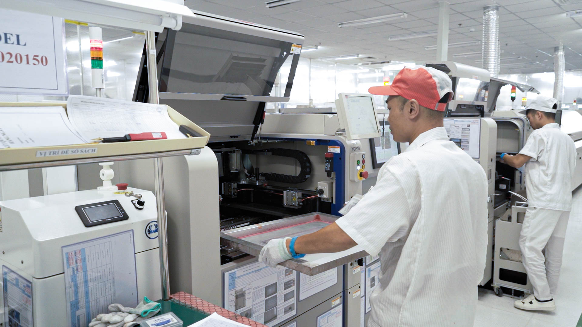
For SMT assembly, solder paste is deposited onto the PCB pads through a stencil.
The solder paste provides:
- Solder alloy for the final joint
- Flux for oxide removal and wetting
- Temporary holding force before reflow
Printing is one of the most influential stages in the entire SMT assembly process. If too little paste is printed, the board may develop open or weak solder joints. Excess paste can contribute to bridging, solder balls or component movement.
Important printing variables include:
- Stencil thickness
- Aperture dimensions
- Squeegee pressure
- Print speed
- Board support
- Stencil-to-board alignment
- Separation speed
- Solder paste condition
- Under-stencil cleaning frequency
SHDC’s profile lists a Yamaha YCP10 solder paste printer. The installed-equipment information states a panel range of approximately 50 × 50 mm to 460 × 510 mm and panel thickness from 0.4 to 3.0 mm. Yamaha’s official YCP10 specifications similarly describe the machine as a compact printer supporting large PCBs and multiple stencil formats. (Yamaha Motor Global Site)
These equipment limits should be treated as machine specifications, not automatic confirmation that every PCB within the range is ready for production. Stencil design, panel support, component density and board warpage still require DFM review.
Step 3: 3D Solder Paste Inspection
Solder paste inspection takes place before components are mounted.
A 3D SPI system can evaluate characteristics such as:
- Paste volume
- Deposit height
- Printed area
- Positional offset
- Insufficient paste
- Excess paste
- Possible bridging between adjacent pads
Detecting a printing problem at this stage is more efficient than discovering it after placement and reflow. Once components have been soldered, correction may require manual rework or board scrapping.
SHDC’s profile lists the Yamaha YSi-SP 3D SPI system. Yamaha states that the YSi-SP inspection machine combines 2D and 3D measurement and supports statistical processing of inspection data. The specific inspection coverage and production settings used by SHDC should still be defined by product and customer requirements. (Yamaha Motor Global Site)
SPI does not correct a print defect by itself. Its value comes from connecting inspection results with actions such as stencil cleaning, paste-condition checks or printing-parameter adjustment.
Step 4: SMT Component Placement
After solder paste inspection, the PCB enters the component placement stage.
During placement:
- Feeders supply components to the machine.
- Cameras identify component geometry and PCB fiducials.
- The placement head picks each component.
- The machine rotates and positions it according to the placement file.
- The component is placed onto the printed solder paste.
SHDC’s profile lists Yamaha YSM20R and YSM10 surface mounters.
The documented YSM20R configuration includes a 95,000 CPH head specification and PCB dimensions up to 810 × 490 mm. Yamaha’s YSM20R technical specifications clarify that rated speed and placement capability depend on the installed head, component type and Yamaha-defined optimum conditions. (Yamaha Motor Global Site)
The YSM10 is listed with a 46,000 CPH head specification and PCB dimensions up to 510 × 460 mm. Yamaha’s official YSM10 specifications state that the rated 46,000 CPH performance is measured under optimum conditions. (Yamaha Motor Global Site)
Actual production throughput will normally be lower than the equipment’s nominal rating because it is affected by:
- Number of components per PCB
- Feeder arrangement
- Component package mix
- Board dimensions
- Placement travel
- Changeover time
- Inspection requirements
- Machine utilization
Placement quality also depends on controlled BOM data, feeder verification, component polarity, package-library accuracy, nozzle selection and first-piece approval.
Step 5: Reflow Soldering
After placement, the PCB passes through the reflow oven.
A typical reflow profile includes:
- Preheat
- Thermal soak
- Time above liquidus
- Peak temperature
- Controlled cooling
During reflow, solder paste melts, wets the pads and component terminations, and forms permanent electrical and mechanical connections.
SHDC’s equipment list includes a JT nitrogen reflow oven. Nitrogen can help reduce oxidation during soldering, but whether it is required depends on the alloy, flux, component finishes and product requirements.
There is no universal reflow profile for every PCB. The correct profile depends on:
- Solder paste
- PCB thickness
- Copper distribution
- Component thermal mass
- Panelization
- Package-temperature limits
- Lead-free or leaded soldering requirements
For projects using Pb-free alloys, SHDC’s guide to lead-free PCB assembly provides more detail on alloy selection and thermal profiling.
A profile should be measured on the actual assembly rather than inferred only from oven zone settings.
Step 6: Automated Optical Inspection and Repair
After reflow, automated optical inspection evaluates the assembled PCB for visible defects.
Depending on the machine program, lighting and component geometry, AOI may identify:
- Missing components
- Incorrect polarity
- Rotation errors
- Placement offset
- Lifted leads
- Visible solder bridges
- Certain insufficient or excessive solder conditions
- Incorrect components with distinguishable visible features
SHDC’s profile lists the Yamaha YSi-V 3D AOI system. Yamaha describes the YSi-V inspection platform as combining two-dimensional inspection, optional three-dimensional inspection and angled imaging. (Yamaha Motor Global Site)
AOI is valuable, but it does not verify everything. It generally cannot confirm:
- Internal BGA solder joints
- Firmware operation
- Complete electrical performance
- Hidden intermittent faults
- Long-term solder-joint reliability
That is why AOI should be part of a broader PCB assembly quality control plan rather than treated as a replacement for electrical testing.
Boards flagged by AOI require review to separate actual defects from false calls. Confirmed defects may be transferred to a controlled repair station and reinspected according to the applicable work instruction. The PCB rework process should define component replacement, cleaning, solder acceptance and post-rework testing.
Step 7: DIP and Through-Hole Assembly
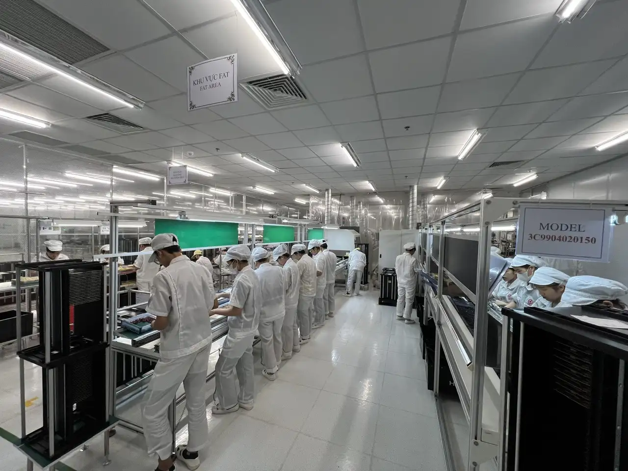
Some electronic products cannot be assembled using SMT alone.
Through-hole assembly is commonly used for:
- Large connectors
- Transformers
- Relays
- Power components
- Electrolytic capacitors
- Mechanical switches
- Components requiring additional mechanical retention
The component leads are inserted through plated holes in the PCB. SHDC’s profile shows AV plug-in equipment, component insertion machines, an LED forming machine and hand-insertion operations.
Automated insertion can improve repeatability for compatible component types, while manual insertion may be required for unusual packages, low-volume products or complex mechanical arrangements.
The choice between surface mounting and through-hole assembly is explained further in SHDC’s comparison of SMT and through-hole assembly.
Common insertion risks include:
- Wrong component
- Incorrect polarity
- Bent leads
- Incomplete seating
- Incorrect component height
- Damage to plated holes
- Mechanical interference with the enclosure
Step 8: Flux Application and Wave Soldering
After through-hole components are inserted, their leads must be soldered.
The process typically includes:
- Flux application
- Preheating
- Contact with the solder wave
- Cooling
- Inspection
Flux supports oxide removal and solder wetting. Its type, application volume and compatibility must be controlled.
SHDC’s profile lists a JT wave soldering machine and shows flux application followed by automatic soldering in its production process.
Potential through-hole soldering defects include:
- Insufficient hole fill
- Solder bridges
- Solder skips
- Icicles
- Non-wetting
- Excess solder
- Lifted pads
- Damaged component leads
Process and acceptance criteria may be defined using customer documentation and relevant industry standards. IPC J-STD-001J addresses materials, methods and acceptance criteria for soldered electronic assemblies, while IPC-A-610J provides post-assembly visual acceptance criteria. IPC notes that the two standards are commonly used together. (shop.ipc.org)
The applicable IPC class should be specified by the customer rather than assumed for every project.
Step 9: ICT and Functional Testing
Optical inspection confirms visible assembly conditions, but it does not prove that the circuit functions correctly.
In-Circuit Testing
ICT can be configured to check:
- Opens and shorts
- Circuit continuity
- Selected resistor or capacitor values
- Diodes and semiconductor junctions
- Certain component-level electrical conditions
SHDC’s profile lists the Kyoritsu ICT F-2000 Plus.
ICT coverage depends on the circuit design, test-point access, fixture and test program. A board with limited test access may not support the same coverage as one designed for automated testing.
Functional Circuit Testing
FCT powers or stimulates the assembly and checks whether it performs its intended functions.
Depending on the product, FCT may verify:
- Power-up behavior
- Inputs and outputs
- Communication interfaces
- Sensors
- Relays
- Displays
- Firmware interaction
- Product-specific operating modes
SHDC’s equipment portfolio also shows functional testing, high-voltage testing, A/V testing and aging-test equipment. The test methods applied to a specific order depend on the product and approved test plan.
ICT and FCT are complementary rather than interchangeable. SHDC’s guide to in-circuit testing versus functional testing explains the difference in more detail.
Step 10: OQC, Packaging and Finished Product Storage
After assembly and testing, accepted products proceed to outgoing quality control.
Depending on customer requirements, OQC may confirm:
- Product identity
- PCB revision
- Quantity
- Visual condition
- Test status
- Labeling
- Packaging
- Required documentation
Packaging should protect the assembly during storage and transportation. Requirements may include:
- ESD-safe bags or trays
- Board separation
- Moisture protection
- Lot identification
- Barcode or serial labels
- Customer-specific packaging
- Protection for international shipping
The completed products are then transferred to the finished-product warehouse before shipment release.
Current PCB Assembly Capabilities at SHDC
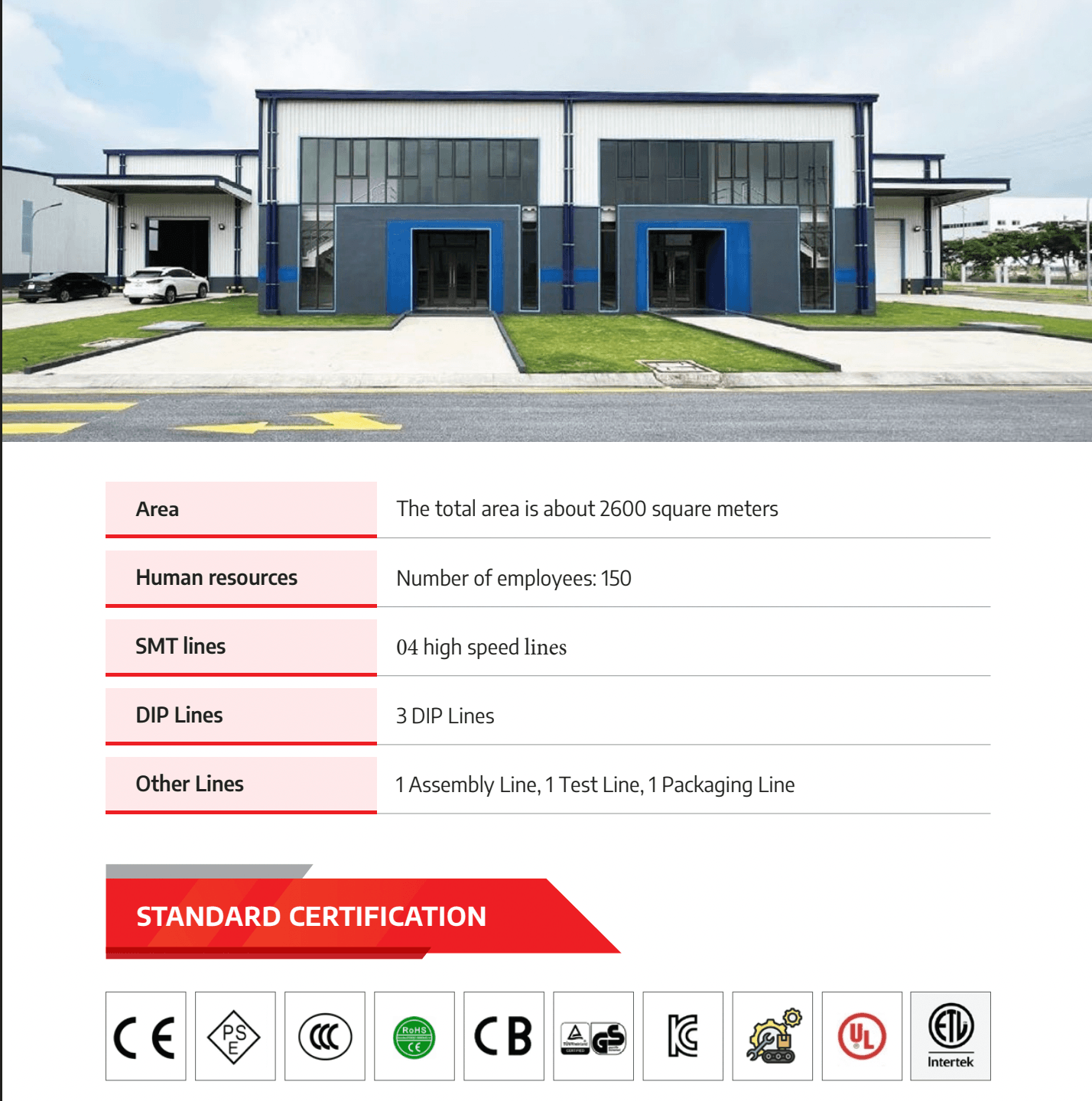
SHDC’s current company profile lists:
- Approximately 2,600 m² of factory area
- Approximately 150 employees
- Four high-speed SMT lines
- Three DIP lines
- One assembly line
- One test line
- One packaging line
The equipment portfolio includes solder paste printing, 3D SPI, Yamaha placement machines, nitrogen reflow, 3D AOI, wave soldering, ICT and functional testing.
The profile separately presents a Phase 2 factory planned for March 2027. Its proposed 28 lines, 1,000-person workforce and 50-million-unit annual output should not be represented as current production capacity.
What US OEMs Should Provide Before PCB Assembly
A complete manufacturing package reduces quotation uncertainty and production risk.
OEMs should normally provide:
- Gerber or ODB++ files
- Fabrication drawing
- BOM with manufacturer part numbers
- Approved component alternates
- Pick-and-place data
- Assembly drawings
- PCB stack-up and surface finish
- Soldering requirements
- Customer or IPC acceptance criteria
- Programming files
- ICT and FCT requirements
- Test procedures and pass/fail limits
- Labeling or serialization requirements
- Packaging instructions
- Prototype quantity and annual forecast
The PCBA manufacturer Vietnam RFQ checklist provides a more detailed list of files and commercial information required for an accurate quotation.
>>>Read more: Power Electronics Manufacturing in Vietnam – SHDC
Conclusion
The PCB assembly process should be evaluated as one connected manufacturing system rather than a collection of individual machines.
At SHDC, the documented process links incoming inspection, solder paste printing, 3D SPI, SMT placement, reflow, AOI, DIP insertion, wave soldering, ICT, FCT, OQC and packaging.
Each stage controls a different risk:
- IQC controls material errors.
- SPI controls solder paste printing.
- Placement controls component identity and position.
- Reflow and wave soldering create electrical connections.
- AOI identifies visible defects.
- ICT checks circuit-level conditions.
- FCT verifies product operation.
- OQC confirms final release requirements.
US OEMs evaluating an EMS partner in Vietnam should therefore review not only nominal machine speed but also data control, inspection coverage, testing strategy, rework procedures and change management.
A controlled process from IQC to final testing provides a stronger foundation for moving a product from prototype builds into stable production.
Frequently Asked Questions
What are the main PCB assembly process steps?
The main stages are incoming inspection, solder paste printing, SPI, SMT placement, reflow, AOI, through-hole insertion, wave soldering, ICT, FCT, OQC and packaging. The exact route depends on the product.
What is the difference between SMT and DIP?
SMT components are mounted directly onto the PCB surface. DIP or through-hole components have leads inserted through plated holes and soldered on the opposite side.
What is the difference between AOI, ICT and FCT?
AOI checks visible assembly conditions. ICT evaluates circuit connections and selected components. FCT verifies whether the assembled board performs its intended functions.
Does every PCB require both ICT and FCT?
No. Testing coverage depends on board design, test access, production volume, product risk and customer requirements.
Does SHDC support both SMT and DIP assembly?
SHDC’s current company profile lists four high-speed SMT lines and three DIP lines, together with assembly, testing and packaging operations.
