
 Tiếng Việt
 日本語
日本語
Lead free PCB assembly is now a standard requirement for many electronics products sold across international markets. However, replacing traditional tin-lead solder with a lead-free alloy is not simply a material substitution.
Lead-free soldering changes the thermal demands placed on the PCB, components, solder paste and manufacturing equipment. It can also narrow the acceptable process window, making accurate printing, thermal profiling, inspection and traceability increasingly important.
For US OEMs outsourcing PCB assembly, the quality of a lead-free product depends on three connected decisions:
- Selecting an alloy that fits the product and manufacturing process.
- Developing a reflow profile for the actual PCB assembly.
- Controlling materials and process variables throughout production.
This guide explains how those decisions affect solder joint quality, manufacturing yield and long-term product reliability.
What Is Lead-Free PCB Assembly?
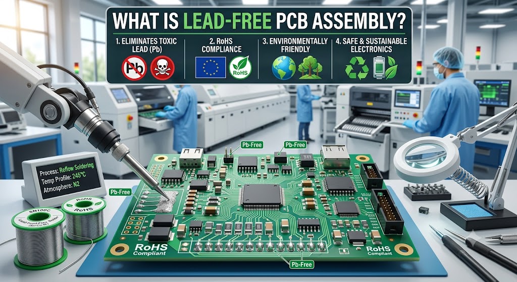
Lead-free PCB assembly is the process of mounting and soldering electronic components onto a printed circuit board without using the conventional tin-lead solder systems historically applied in electronics manufacturing.
The term covers more than SMT reflow. A complete lead-free assembly may involve:
- Solder paste printing
- Surface-mount component placement
- Reflow soldering
- Wave or selective soldering
- Through-hole component insertion
- Hand soldering and rework
- Inspection and electrical testing
- Material and process traceability
IPC J-STD-001 establishes materials, methods and verification criteria for producing soldered electrical and electronic assemblies, including both leaded and lead-free interconnections. IPC-A-610 is commonly used alongside it to define visual acceptance criteria for completed assemblies.
Lead-Free Does Not Automatically Mean RoHS Compliant
“Lead-free” and “RoHS compliant” are related terms, but they should not be treated as exact synonyms.
Lead-free normally describes a solder alloy or assembly process that does not use conventional lead-bearing solder. RoHS compliance applies to restricted substances across the product’s homogeneous materials, subject to the directive’s scope, concentration limits and applicable exemptions.
The European Union’s RoHS Directive currently restricts ten substances in electrical and electronic equipment, including lead, mercury, cadmium and hexavalent chromium. Therefore, using lead-free solder alone does not establish compliance for the entire finished product.
An OEM should also review:
- PCB laminate and surface-finish declarations
- Component material declarations
- Cable, connector and enclosure materials
- Applicable RoHS exemptions
- Supplier certificates of conformance
- BOM-level compliance documentation
Why Lead-Free Assembly Matters to US OEMs
Not every electronic product sold in the United States is automatically subject to the EU RoHS Directive. Nevertheless, many US manufacturers specify lead-free and RoHS-aligned production because their products may be sold in Europe or supplied to global customers.
A consistent lead-free strategy can help an OEM:
- Support multi-market product launches
- Meet customer restricted-substance requirements
- Standardize manufacturing between suppliers
- Reduce future redesign and requalification work
- Maintain clearer material documentation across the BOM
- Avoid mixing incompatible leaded and lead-free processes
The requirement should be defined during the RFQ and NPI stages rather than added after the production process has already been developed.
Common Solder Alloys Used in Lead-Free PCB Assembly
There is no single solder alloy that is suitable for every application. Selection should be based on the product environment, component finishes, expected reliability, assembly method and available process window.
IPC J-STD-006 defines requirements, nomenclature and test methods for electronic-grade solder alloys and solder products.
SAC305 Solder Alloy
SAC305 is one of the most widely recognized lead-free solder alloys. Its nominal composition is:
- 96.5% tin
- 3.0% silver
- 0.5% copper
It is used in solder paste, wire and bar formats and can be applied in SMT reflow, hand soldering, selective soldering and wave soldering. Its liquidus is approximately 220°C, although the required reflow peak for a finished assembly will be higher and must follow the selected paste specification.
SAC305 is often considered because it has:
- Broad material availability
- Established process knowledge
- Compatibility with many lead-free components and finishes
- Extensive historical use across electronics manufacturing
However, its silver content affects material cost, while its higher processing temperature compared with traditional SnPb solder increases the importance of PCB and component thermal compatibility.
>>>Read more: PCBA Manufacturer Vietnam RFQ Checklist for US OEMs
Low-Silver SAC Alloys
Low-silver alloys such as SAC105 and SAC0307 reduce the silver content relative to SAC305. Depending on the formulation, they may be considered for cost-sensitive products, portable electronics or specific mechanical reliability requirements.
Reducing silver content changes the alloy’s melting behavior and mechanical characteristics. A low-silver alloy should not automatically be treated as a drop-in replacement for SAC305 without validating wetting, thermal cycling, mechanical shock and production yield. Solder suppliers therefore provide flux systems and alloy formulations designed specifically for low-silver processing.
Tin-Copper Alloys
Tin-copper systems are frequently evaluated for wave soldering, selective soldering and applications where silver cost is a concern.
Potential process considerations include:
- Slower wetting than some silver-containing alloys
- Copper dissolution
- Solder-pot composition control
- Dross generation
- Bridging performance
- Compatibility with board and component finishes
The correct decision depends on the assembly rather than alloy price alone. Both SAC305 and silver-free or low-silver alternatives can be appropriate when selected for a defined product and process.
Bismuth-Based Low-Temperature Alloys
Bismuth-containing alloys allow manufacturers to reduce reflow temperature. They may be considered for:
- Heat-sensitive components
- Assemblies with significant package warpage
- Multilayer boards exposed to thermal stress
- Energy-sensitive production processes
- Products requiring a lower peak temperature
Some commercial bismuth-tin systems can be reflowed well below typical SAC temperatures. However, their joint properties, component-finishing compatibility and reliability profile must be evaluated for the intended application.
Particular care is required when bismuth alloys may interact with lead-bearing component finishes. Solder-material suppliers warn that tin-lead-bismuth combinations can form low-melting phases, making material verification critical before adopting a low-temperature process.
Lead-Free Solder Alloy Comparison
| Alloy family | Typical application | Key advantages | Main considerations |
|---|---|---|---|
| SAC305 | SMT reflow, hand, selective and wave soldering | Established process history and broad availability | Higher silver cost and thermal exposure |
| Low-silver SAC | Consumer, portable and cost-sensitive electronics | Lower silver content and application-specific mechanical performance | Requires product-level qualification |
| Tin-copper | Wave and selective soldering | Lower material cost and no silver | Wetting, copper dissolution and pot control |
| Bismuth-based | Low-temperature SMT assembly | Reduced reflow temperature and thermal stress | Material compatibility and mechanical reliability |
| Doped specialty alloy | Automotive, power or high-reliability products | Properties tailored to specific service conditions | Supplier-specific validation and sourcing |
The most appropriate alloy is not necessarily the one with the lowest melting point or purchase price. The correct choice is the alloy that produces repeatable joints while meeting the product’s mechanical, thermal and regulatory requirements.
>>>Read more: PCBA Vietnam: High-Reliability PCB Assembly Partner for US OEMs
How to Select a Lead-Free Solder Alloy
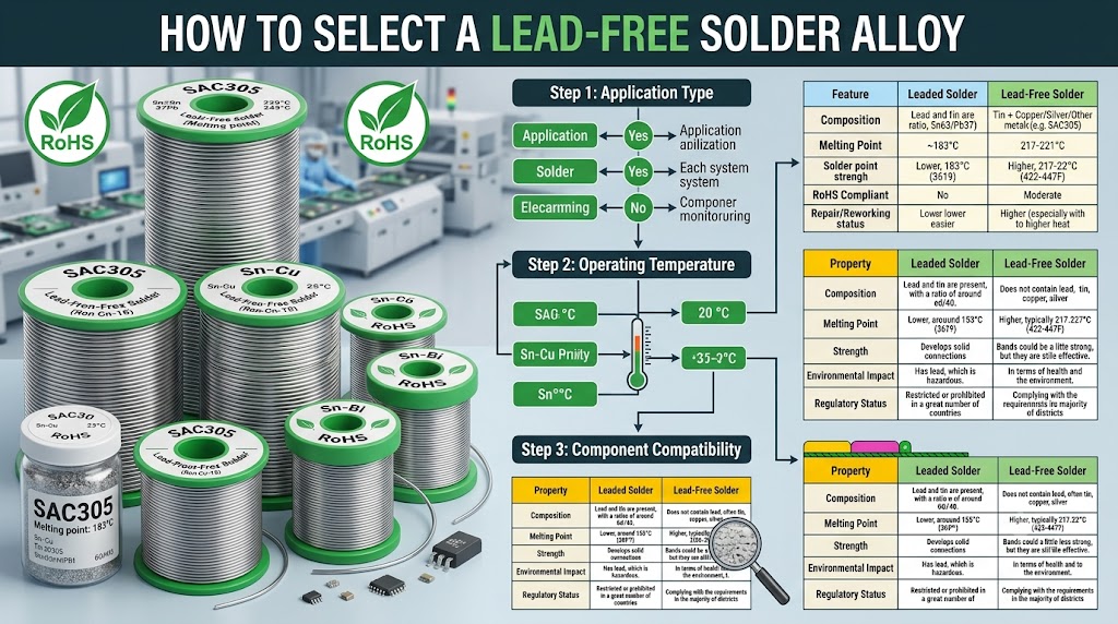
Before approving an alloy, the OEM and assembly manufacturer should jointly review the following factors.
Product Operating Environment
A solder joint used in a desktop consumer product may experience different stresses from one installed in an industrial controller, vehicle or power-conversion system.
The qualification plan should consider:
- Operating-temperature range
- Thermal cycling
- Mechanical shock
- Vibration
- Product life expectancy
- Current and power density
- Humidity and contamination exposure
- Field repair requirements
Reliability should be evaluated against the actual application rather than assumed from the alloy name.
PCB and Component Compatibility
The manufacturer should confirm compatibility between the alloy and:
- PCB surface finish
- Component termination finish
- BGA solder-ball composition
- Copper pad design
- PCB laminate
- Via structures
- Mixed leaded and lead-free components
A mismatch may contribute to poor wetting, weak interfaces, excessive intermetallic growth or an unpredictable mixed-alloy joint.
Manufacturing Process
The approved alloy must work across every soldering stage used on the product.
For example, a mixed-technology board may require:
- SMT reflow on the first side
- A second reflow on the opposite side
- Selective or wave soldering for through-hole parts
- Manual soldering during final assembly
- Rework after inspection or testing
The OEM should confirm whether the same alloy family will be maintained throughout the process and how cross-contamination will be prevented.
Supply-Chain and Cost Factors
Alloy evaluation should also include:
- Paste, wire and bar availability
- Regional supplier support
- Minimum order quantities
- Storage conditions
- Shelf life
- Lot-to-lot traceability
- Prototype-to-production continuity
- Qualification cost
- Material-change notification requirements
A small reduction in solder cost may not provide meaningful savings if it creates additional inspection, qualification or rework requirements.
>>>Read more: SHDC – Trusted Non-China PCBA Manufacturer in Vietnam for U.S. OEMs
Understanding the Lead-Free Reflow Profile
The reflow profile is the temperature history experienced by the PCB and its components as the assembly moves through the oven.
A profile is not simply a list of oven zone settings. It must be measured on the actual board using thermocouples placed at representative solder joints and thermally significant locations.
IPC-7530 provides guidance for developing thermal profiles for leaded and lead-free mass-soldering processes.
Why There Is No Universal Lead-Free Reflow Profile
Different boards respond differently to the same oven recipe because of variations in:
- PCB dimensions and thickness
- Copper distribution
- Number of layers
- Panelization
- Component size
- Thermal mass
- Package type
- Component density
- Oven loading
- Conveyor speed
The solder paste supplier’s recommended profile should be used as the starting process window. Adjustments may then be required for the board design and production equipment.
For example, one SAC305 paste specification provides a recommended time above liquidus of 45–60 seconds and a thermocouple-measured peak range of 230–260°C, while also stating that all parameters are references that may need modification for the product and process. These values must not be copied as a universal recipe for every lead free PCB assembly.
Preheat and Ramp
During preheat, the assembly temperature rises in a controlled manner.
The objective is to:
- Reduce thermal shock
- Begin solvent evaporation
- Support flux activation
- Limit temperature differences across the assembly
- Prepare the board for the liquidus phase
An excessive heating rate can contribute to solder balling, component damage or uneven temperature distribution. A very slow ramp may consume flux activity before the joint reaches the soldering stage.
Soak Zone
A soak zone can help reduce the temperature difference between low-mass and high-mass areas of the board.
It may be useful when an assembly contains:
- Large connectors
- Shielding
- Heavy copper areas
- Small passive components
- BGAs or QFNs
- Mixed package sizes
However, an unnecessarily long soak can increase oxidation or exhaust the flux prematurely. Ramp-to-peak and ramp-soak-spike profiles can both be effective when matched to the paste and board.
Time Above Liquidus
Time above liquidus, commonly abbreviated as TAL, is the period during which the solder alloy remains above its liquidus temperature.
If TAL is too short, the assembly may experience:
- Incomplete reflow
- Insufficient wetting
- Cold or poorly formed joints
- Incomplete coalescence
If it is excessive, potential risks include:
- Flux exhaustion
- Excessive intermetallic growth
- Component or laminate damage
- Increased oxidation
- Unwanted joint-shape changes
TAL should be measured at the solder joint, not inferred solely from the oven-program settings.
Peak Temperature
Peak temperature must be high enough to achieve full solder reflow and wetting, but low enough to protect the PCB and components.
The process engineer must consider:
- Paste supplier recommendations
- Component package limits
- PCB laminate capability
- Moisture sensitivity
- Number of thermal cycles
- Temperature variation across the board
The hottest and coldest monitored joints must both remain inside the approved process window.
Controlled Cooling
Cooling rate affects solder-joint microstructure and the thermal stress experienced by the assembly.
A controlled cooling stage can support:
- Consistent joint formation
- Fine-grain structure
- Reduced thermal shock
- Stable board handling after reflow
The acceptable rate should come from the paste specification and product qualification rather than an assumed factory-wide value.
Reflow Profile Control Points
| Profile stage | Main parameter | Risk when insufficient | Risk when excessive |
|---|---|---|---|
| Ramp/preheat | Temperature-rise rate | Poor flux activation or uneven heating | Thermal shock and solder balling |
| Soak | Time and temperature range | High temperature difference across PCB | Oxidation and flux exhaustion |
| Time above liquidus | Time over alloy liquidus | Incomplete wetting or reflow | Excessive intermetallic growth |
| Peak | Maximum joint temperature | Cold or incomplete joints | PCB or component damage |
| Cooling | Temperature-fall rate | Coarse joint structure | Thermal stress or warpage |
How to Develop a Reflow Profile for an Actual PCB

A practical profiling process normally includes the following steps:
- Review the solder paste technical data sheet.
- Identify the alloy liquidus and recommended process window.
- Select thermally significant measurement locations.
- Attach thermocouples directly to representative solder joints.
- Include large, small, shielded and temperature-sensitive components.
- Run the instrumented profile board through the oven.
- Compare ramp rate, soak, TAL, peak and cooling with the approved limits.
- Adjust conveyor speed and oven zones.
- Repeat the profile until all monitored locations are within the process window.
- Approve and store the profile against the assembly part number and revision.
A new profile or verification run may be required following changes to:
- PCB design or thickness
- Panel dimensions
- Copper distribution
- Component package
- Solder paste
- Alloy
- Oven
- Conveyor speed
- Production loading
- Component substitution
Process Control for Reliable Lead-Free PCB Assembly
A stable reflow profile cannot compensate for uncontrolled solder paste, poor stencil printing or incorrect component handling. Reliable lead-free production depends on controlling the full process.
Incoming Material and BOM Control
Incoming quality control should confirm that the received material matches the approved manufacturing data.
Key controls include:
- Manufacturer part number verification
- Component package and value
- Date and lot code
- Termination finish
- Moisture-sensitivity status
- PCB revision
- Surface finish
- Material declaration
- Approved-substitute status
Any component substitution that changes termination finish, thermal mass or package geometry may affect the soldering process and should pass engineering review.
Solder Paste Storage and Preparation
Solder paste performance depends on handling before it reaches the stencil.
The manufacturer should control:
- Refrigerated storage
- First-in, first-out usage
- Lot traceability
- Controlled thawing
- Container opening time
- Stencil life
- Temperature and humidity
- Paste replenishment
- Disposal criteria
The paste supplier’s technical data sheet should be the controlling reference. Procedures should not rely on generic handling times that are applied to every product.
Stencil Design and Solder Paste Printing
Printing is one of the most influential stages in SMT assembly because the solder deposit establishes the volume available to form the joint.
Important variables include:
- Stencil thickness
- Aperture dimensions
- Area ratio
- Aperture shape
- Step-stencil requirements
- Squeegee pressure and speed
- Separation speed
- Board support
- Under-stencil cleaning
- Paste condition
QFN thermal pads, bottom-terminated components and fine-pitch devices often require aperture designs that balance solder volume, release efficiency and voiding risk.
Solder Paste Inspection
Three-dimensional solder paste inspection can measure:
- Paste volume
- Height
- Area
- Offset
- Insufficient deposits
- Excess deposits
- Bridging
- Shape variation
The greatest value of SPI is not only defect detection. Its data can be used to identify print-process drift before the defect reaches placement and reflow.
Placement Control
Placement accuracy depends on correct manufacturing data and machine setup.
Controls should cover:
- Feeder verification
- Component identity
- Package library
- Polarity
- Rotation
- Nozzle selection
- Pickup position
- Placement force
- Fiducial recognition
- First-piece approval
For small passives, uneven paste deposits or placement offsets can increase the likelihood of tombstoning during reflow.
Reflow Oven Control
Once an oven recipe has been approved, it must remain controlled.
The manufacturer should define:
- Recipe access and revision control
- Conveyor-speed verification
- Zone-temperature monitoring
- Alarm limits
- Oven maintenance
- Profile-verification frequency
- Product changeover procedure
- Nitrogen-flow control where applicable
- Reaction plan for an out-of-control result
The approved profile must be connected to the correct product revision rather than stored as an undocumented machine setting.
Inspection and Electrical Testing
Each inspection method covers a different risk.
SPI evaluates solder paste before component placement.
AOI identifies visible defects such as missing parts, polarity errors, misalignment and certain solder-joint conditions.
X-ray inspection supports analysis of hidden joints under BGA, QFN and similar packages.
ICT checks electrical connectivity and selected component values.
FCT verifies whether the assembled board performs its intended functions.
No single method detects every possible manufacturing defect. Inspection and testing coverage should therefore be selected according to board complexity, component technology and product risk.
Traceability, SPC and Change Control
Useful process indicators may include:
- First-pass yield
- Rework rate
- Defect rate by process stage
- SPI and AOI trends
- Top defect categories
- Test failure modes
- Solder paste lot
- Component lot
- PCB lot
- Machine-program revision
- Reflow recipe and profile record
- Operator and production time
Trend data is more valuable than a pass/fail report alone because it helps identify gradual process drift.
Common Lead-Free Soldering Defects
| Defect | Common contributing factors | Recommended process checks |
|---|---|---|
| Tombstoning | Unequal pad heating, paste imbalance, component offset | Pad design, SPI results, placement and profile |
| Solder bridging | Excess paste, poor aperture design, misalignment | Stencil, print volume and placement data |
| Non-wetting | Oxidation, contamination, insufficient heat | Material storage, surface finish and profile |
| Solder balls | Paste slump, rapid heating, excessive deposit | Paste handling, printing and ramp rate |
| Voiding | Trapped volatiles, pad design or profile conditions | Paste, aperture design, soak and X-ray |
| Head-in-pillow | BGA warpage, oxidation or inadequate contact | Component condition, placement and thermal profile |
| Graping | Oxidation of small deposits and inadequate flux protection | Paste type, aperture size and profile |
| Delamination | Moisture, laminate limitations or excessive thermal exposure | PCB storage, MSL handling and peak temperature |
A defect should not be corrected by changing one machine setting without identifying the underlying cause. A structured review should connect the defect to material, design, printing, placement, reflow or handling data.
DFM Considerations for Lead-Free PCB Assembly
Design for manufacturability should begin before stencil fabrication or production programming.
PCB Laminate Capability
A lead-free board may experience higher thermal exposure than a comparable SnPb assembly. The OEM should review:
- Glass-transition temperature
- Decomposition temperature
- Z-axis expansion
- Number of reflow cycles
- Board thickness
- Copper balance
- Via reliability
- Delamination resistance
Pad and Stencil Design
The design review should address:
- Symmetrical passive-component pads
- Solder-mask definition
- Thermal relief
- Fine-pitch aperture ratios
- QFN thermal-pad segmentation
- Via-in-pad treatment
- BGA escape routing
- Copper-density imbalance
- Minimum spacing
- Board support during printing
Moisture-Sensitive Components
Moisture absorbed by a component package can expand rapidly during reflow and cause internal package damage.
The manufacturing process should define:
- Moisture-sensitivity level
- Floor-life tracking
- Dry-cabinet storage
- Moisture-barrier bag control
- Humidity-indicator card checks
- Baking requirements
- Resealing procedure
Double-Sided and Mixed-Technology Boards
Boards requiring two reflow cycles need special review because components and solder joints on the first side are exposed again during second-side processing.
The manufacturer should evaluate:
- Component weight
- Joint surface tension
- Second-side support
- Thermal exposure
- Process sequence
- Adhesive requirements
- Selective soldering access
- Manual soldering risk
What US OEMs Should Include in a Lead-Free PCBA RFQ
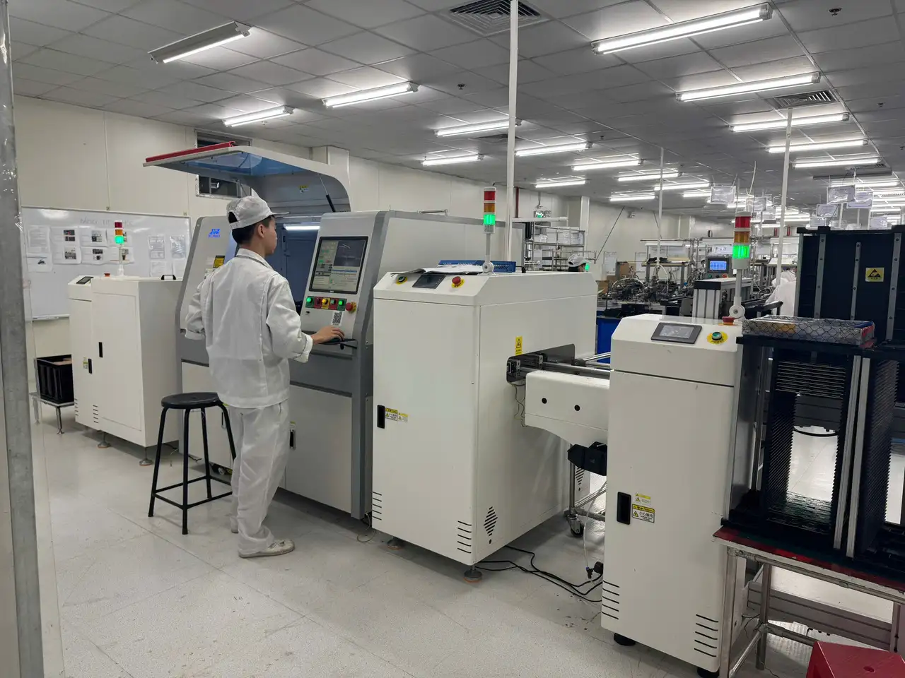
A detailed RFQ allows the manufacturer to evaluate technical risk before quoting.
The data package should include:
- Gerber or ODB++ files
- Fabrication drawing
- PCB stack-up
- Surface-finish requirement
- Complete BOM with manufacturer part numbers
- Approved alternates
- Pick-and-place data
- Assembly drawings
- Solder-alloy requirement
- Flux and cleaning requirement
- IPC product class
- RoHS and material-compliance requirements
- Inspection criteria
- X-ray requirements
- ICT or FCT specifications
- Programming instructions
- Serial-number and traceability requirements
- Conformal-coating requirements
- Pilot quantity
- Annual forecast
- Packaging and shipping requirements
OEMs should also ask the potential supplier:
- Is the reflow profile developed for each PCB assembly?
- Can the supplier provide a thermal-profile record?
- Which solder alloys and paste systems are available?
- How are solder paste and component lots traced?
- What SPI and AOI controls are used?
- How are BGA and QFN joints inspected?
- What happens when a component substitution is required?
- How are oven recipes and machine programs revision-controlled?
- Which acceptance criteria will apply?
- What data is included in the pilot-build report?
For additional RFQ planning, SHDC’s PCBA pricing guide explains how BOM complexity, assembly method, testing scope, tooling and volume affect quotation accuracy.
Lead-Free PCB Assembly Capabilities at SHDC
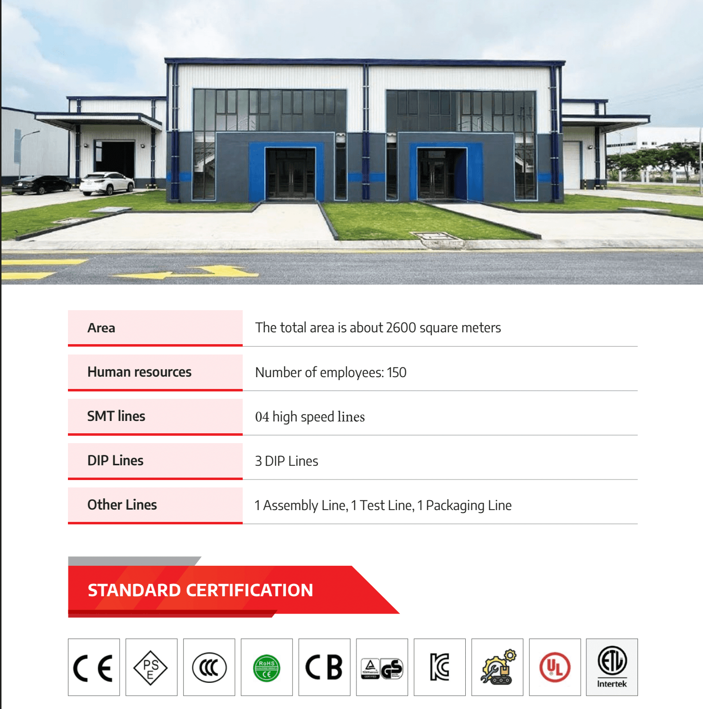
SHDC Electronics provides EMS support covering component soldering, assembly, testing and final packaging. Its current factory profile lists four high-speed SMT lines, three DIP lines, one assembly line, one test line and one packaging line.
The production equipment described in the company profile includes:
- Yamaha YCP10 solder paste printer
- Yamaha YSM20R and YSM10 placement machines
- Yamaha 3D SPI
- Yamaha 3D AOI
- N2 reflow oven
- Wave soldering equipment
- Kyoritsu ICT
- Functional testing
- Visual inspection
- High-voltage and aging tests
SHDC’s documented production flow covers IQC, warehousing, solder paste printing, component mounting, reflow, AOI, repair, ICT, FCT, OQC and packaging. This process structure enables material control, inspection and testing to be integrated into the broader PCBA workflow rather than treated as isolated final checks.
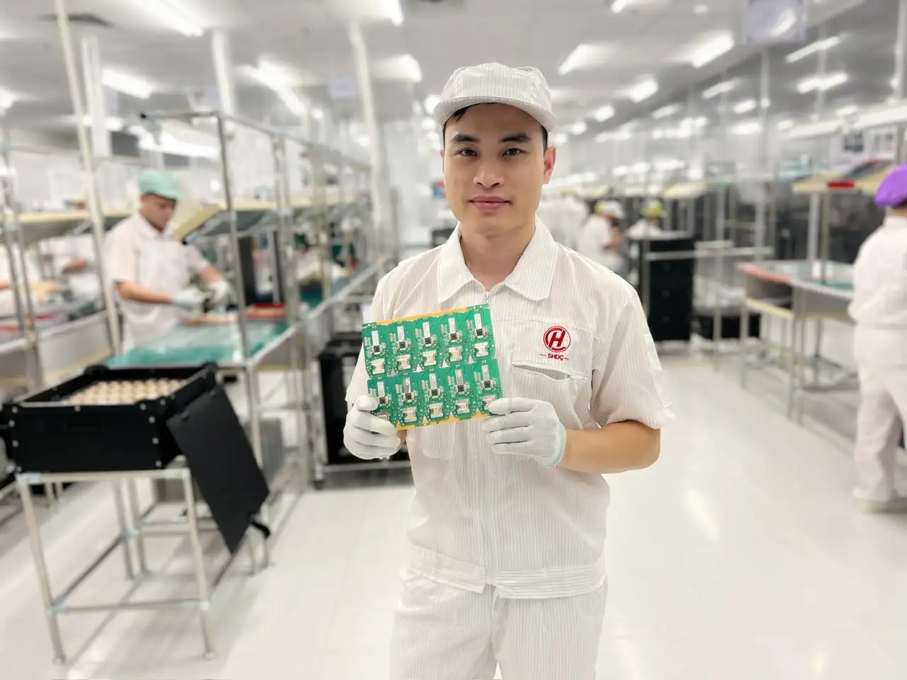
For US OEM programs, the first technical step should be a review of the PCB files, BOM, alloy requirement, component thermal limits and testing scope. The process can then be defined around the actual product rather than a generic lead-free recipe.
For a broader explanation of these manufacturing stages, see SHDC’s guide to the SMT PCBA process.
Lead-Free PCB Assembly Checklist Before a Pilot Build
Before releasing a pilot order, confirm that:
- The solder alloy and paste have been approved.
- PCB and component finishes are compatible.
- RoHS and material requirements are documented.
- Component thermal limits have been reviewed.
- Moisture-sensitive parts have been identified.
- Stencil design has passed DFM review.
- SPI limits have been established.
- Thermocouple locations have been selected.
- The reflow profile has been recorded.
- AOI and X-ray coverage have been defined.
- ICT and FCT requirements are available.
- Acceptance criteria have been agreed.
- Traceability requirements are documented.
- Approved substitutes are controlled.
- Pilot-build results will be reviewed before mass production.
Conclusion
Successful lead free PCB assembly depends on more than choosing a solder marked “Pb-free.”
The solder alloy must fit the product’s operating environment, component finishes and manufacturing sequence. The reflow profile must be measured on the actual board. Printing, placement, material handling, inspection, testing and change control must then keep the process inside its approved window.
For US OEMs, the most useful supplier evaluation question is not simply, “Can you run lead-free solder?”
A better question is:
How will you select, validate, monitor and document the lead-free process for this specific PCB assembly?
A manufacturer that can answer with process records, inspection data, traceability and a structured qualification plan is better positioned to support the transition from prototype to stable production.
Frequently Asked Questions About Lead-Free PCB Assembly
What is lead-free PCB assembly?
Lead-free PCB assembly is the process of mounting and soldering components onto a printed circuit board using alloys that do not rely on conventional tin-lead solder. It can include SMT reflow, wave soldering, selective soldering, hand soldering, inspection and electrical testing.
Is SAC305 suitable for every PCB assembly?
No. SAC305 is widely used, but alloy selection should depend on operating conditions, mechanical requirements, component finishes, soldering method, cost and qualification results.
What temperature is required for lead-free reflow soldering?
There is no universal peak temperature for every lead-free assembly. The correct profile depends on the solder paste specification, alloy, PCB thermal mass and component limits. Peak temperature must be measured on the actual assembly using thermocouples.
Is lead-free the same as RoHS compliant?
No. Lead-free usually describes the solder or soldering process. RoHS compliance covers multiple restricted substances across the homogeneous materials in the finished product and may involve scope and exemption considerations.
Can a tin-lead PCB design be converted directly to lead-free?
Not always. The OEM should review component finishes, PCB laminate capability, surface finish, stencil design, moisture sensitivity and thermal limits before changing the soldering process.
What are the most common lead-free soldering defects?
Common defects include tombstoning, bridging, non-wetting, solder balls, graping, voiding, head-in-pillow and thermal damage. Root causes may originate in design, material handling, printing, placement or reflow.
How can an OEM verify a lead-free process?
The OEM can request material declarations, solder-alloy records, paste lot traceability, reflow-profile data, SPI and AOI reports, test results and process-change documentation.
What files are required for a lead-free PCB assembly quotation?
A complete quotation normally requires Gerber or ODB++ files, BOM, pick-and-place data, assembly drawings, PCB specifications, solder requirements, production volume and inspection and testing requirements.
>>>Read more: Automotive PCBA Vietnam | Trusted Non-China Manufacturer for USA
