Tiếng Việt
 日本語
日本語
PCB panelization is the process of arranging one or more individual circuit boards into a larger manufacturing panel. Instead of processing each PCB separately, the manufacturer moves the full panel through solder-paste printing, component placement, reflow, inspection, testing, and selected downstream operations.
A well-designed panel can improve conveyor handling, equipment alignment, production throughput, and board protection. A poorly designed panel can create warpage, insufficient rigidity, component damage, difficult depanelization, excess material waste, or incompatibility with SMT equipment.
For US OEMs, panelization should not be treated as a last-minute fabrication decision. It should be reviewed with the PCB fabricator and assembly manufacturer before the final production package is released. Panel dimensions, separation method, rail requirements, fiducials, tooling holes, component clearance, and depanelization risks must all match the actual manufacturing process.
Main content
ToggleWhat Is PCB Panelization?
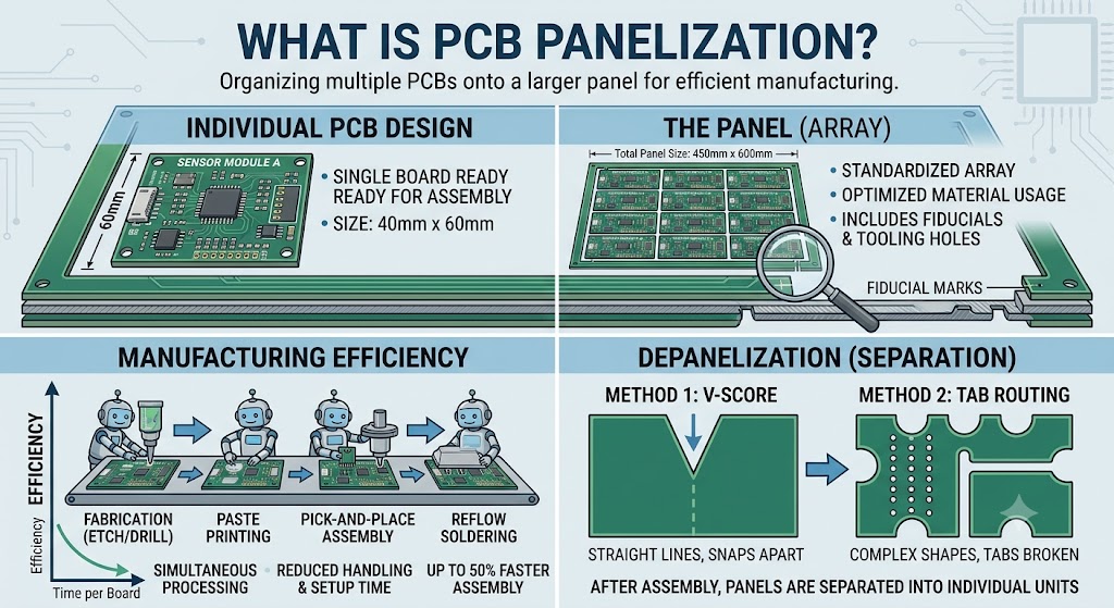
PCB panelization combines multiple individual PCBs, or multiple copies of the same PCB, into one larger array for manufacturing and assembly.
A production panel may contain:
- Several identical PCBs
- Several product variants
- Different small boards used in the same product
- One irregular board surrounded by manufacturing rails
- A single PCB that requires a carrier-style border for conveyor handling
Panelization is used in both bare-board fabrication and PCB assembly, but the objectives are not identical.
During fabrication, the manufacturer may optimize panel utilization around laminate dimensions, tooling, plating, imaging, drilling, and routing. During assembly, the panel must also work with stencil printers, pick-and-place machines, reflow ovens, AOI equipment, conveyors, fixtures, and depanelization processes.
The IPC-2221B generic printed board design standard includes guidance related to printed-board panelization, palletization, and fiducial clearance. However, the final design must also follow the selected manufacturer’s equipment and process requirements.
OEMs should therefore distinguish between:
- Fabrication panelization, optimized primarily for bare-PCB manufacturing
- Assembly panelization, optimized for SMT, inspection, testing, and handling
- Shipping panelization, where boards may remain connected for protection or downstream assembly
A panel that works well for fabrication may still require changes before it is suitable for automated assembly.
Why Is PCB Panelization Used?
Panelization can provide several manufacturing benefits.
More stable conveyor handling
Small, narrow, round, or irregularly shaped PCBs may not travel reliably through standard conveyor systems. Tooling rails or surrounding panel material can create consistent edges for transport through the SMT line.
Higher production throughput
Multiple boards can pass through printing, placement, reflow, and inspection in one cycle. This can reduce handling time per PCB and increase equipment utilization.
Improved alignment
Panel-level fiducials and tooling features help machines identify the panel position and compensate for offset or rotation.
Protection for small boards
The surrounding panel structure can reduce direct handling of individual boards before assembly is completed.
Easier process standardization
A manufacturer may use standardized panel dimensions or orientations across product families to simplify equipment setup, storage, carriers, and process documentation.
Panelization is not automatically beneficial in every case. Additional laminate, routing, rails, tabs, and depanelization work may increase cost. The design should balance manufacturing efficiency against material usage and separation risk.
When Is PCB Panelization Required?
PCB panelization is commonly considered when:
- The individual PCB is too small for conveyor handling
- The board has curved or irregular edges
- Several boards must be assembled together as one set
- Production volume makes multi-up processing more efficient
- The design requires tooling rails
- The assembly has components extending beyond the board edge
- The board requires additional rigidity during printing or reflow
- Automated handling systems require standardized dimensions
- Fiducials or tooling holes cannot fit on the individual PCB
- Testing or final assembly is easier while boards remain connected
A large rectangular PCB may not need multiple boards in one array, but it may still require temporary rails to work with the SMT line.
The panel design should be reviewed during the DFM checklist for PCBA manufacturing, not after fabrication data has already been approved.
Common PCB Panelization Methods
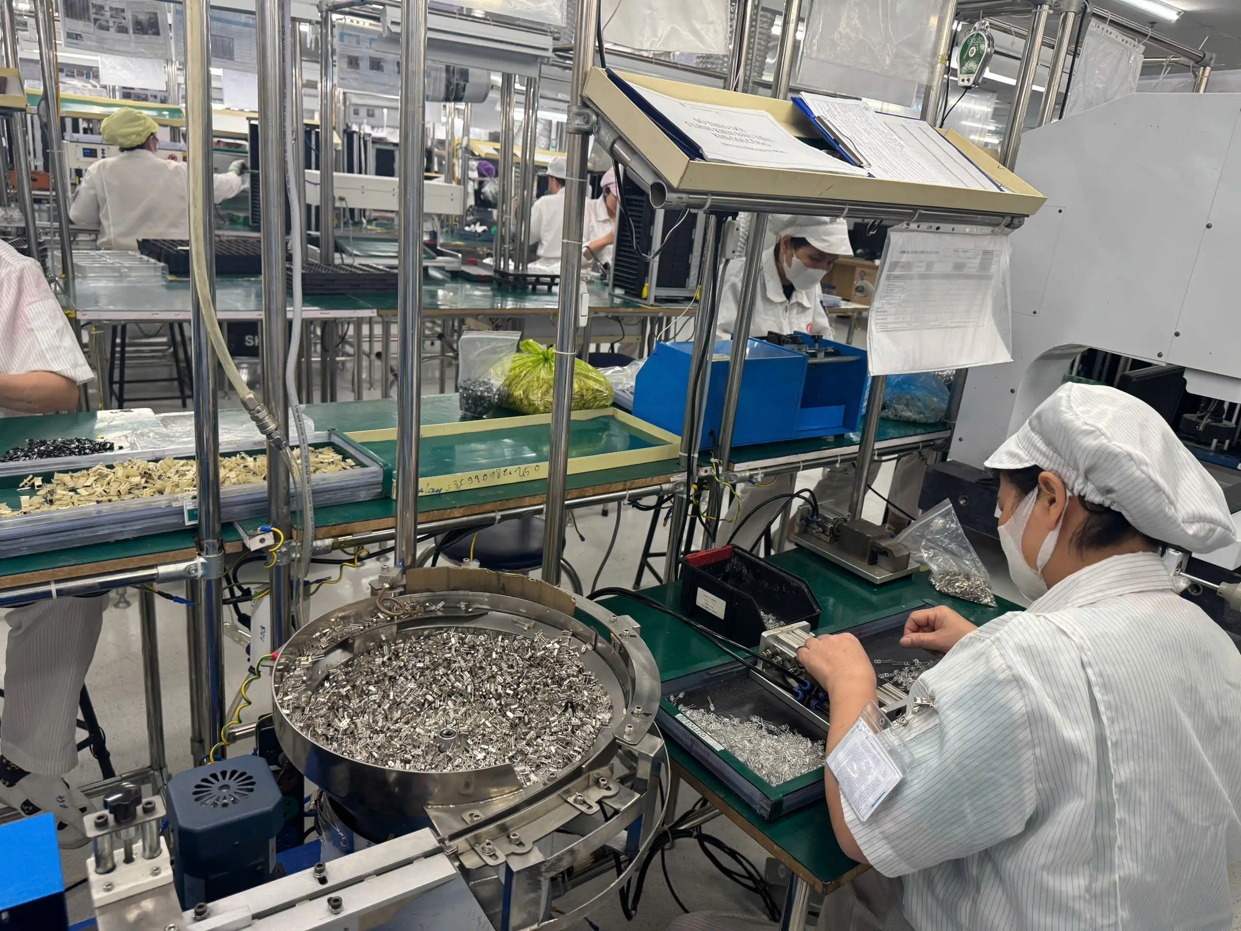
The two most common breakaway approaches are V-scoring and tab routing. They create different restrictions on board geometry, component placement, edge quality, and depanelization.
V-Cut or V-Scoring
V-scoring creates grooves along the top and bottom surfaces of a PCB panel. A controlled amount of material remains between the grooves so the boards stay connected during manufacturing and can later be separated.
V-scoring is generally suitable when:
- Board outlines are rectangular
- Separation lines are straight
- Multiple boards align in rows or columns
- Edge contours do not require complex routing
- Components and copper can be kept away from the score line
V-score lines must normally extend across the relevant panel direction. They are not appropriate for arbitrary curved contours or internal separation shapes.
The score lines should be clearly shown in the panel fabrication drawing. Altium’s guide to creating a PCB panel fabrication drawing recommends documenting V-score lines, tooling requirements, fiducials, and routing information in the released panel documentation.
Advantages of V-scoring
- Straightforward for rectangular board arrays
- Relatively efficient separation
- Limited routing waste between adjacent boards
- Suitable for repetitive rows and columns
- Can support high-volume production
Limitations of V-scoring
- Separation lines generally need to be straight
- Mechanical stress may be transferred into the PCB during breaking
- Components near the score line can be exposed to bending
- The final edge may retain a visible score profile
- Irregular board outlines are difficult or impossible to produce with V-scoring alone
The OEM should confirm the remaining material thickness, score geometry, allowable board thickness, and depanelization equipment with the fabricator.
Tab Routing
Tab routing uses routed slots to separate most of each PCB outline while leaving small connecting tabs between the board and the panel frame or adjacent boards.
It is generally suitable for:
- Irregular board shapes
- Curved outlines
- Boards requiring controlled attachment points
- Arrays where V-score lines cannot extend straight across the panel
- Designs with selected areas that must remain supported
The number, width, and location of tabs influence panel strength and the stress applied during separation.
If tabs are too weak, boards may move or detach prematurely. If they are too strong, depanelization may require excessive force or additional machining.
Mouse bites
Mouse bites are a row of small holes placed across or near a breakaway tab. They reduce the remaining material so the tab can be broken more easily.
Altium describes mouse bites as perforated breakaway connections created by cutouts, holes, and small remaining tabs. The residual material may be trimmed or routed after the PCB is separated.
Mouse bites can leave small projections on the board edge. This may be acceptable for an internal PCB but unsuitable where the edge must fit tightly into an enclosure or remain cosmetically clean.
Routed tabs without mouse bites
Some panel designs use solid tabs that are cut with a router during depanelization. This can provide cleaner edges and lower manual break stress, but it requires appropriate tooling and fixturing.
V-Cut vs. Tab Routing
| Factor | V-Cut | Tab routing |
|---|---|---|
| Board geometry | Best for rectangular boards | Supports complex outlines |
| Separation path | Straight lines | Follows routed contours |
| Material utilization | Often efficient between boards | Requires routing channels |
| Panel rigidity | Depends on score arrangement | Adjustable through tab placement |
| Edge after separation | Scored edge | Routed edge or tab remnant |
| Mechanical stress | Can be significant during breaking | Depends on tab and tool method |
| Component restrictions | Clearance from score line required | Clearance from tabs and router path required |
| Setup complexity | Relatively simple | More routing and tab design decisions |
| Best use case | Repetitive rectangular arrays | Irregular or mechanically sensitive designs |
Neither method is universally better. The correct choice depends on board shape, component placement, allowable stress, production volume, cosmetic requirements, and available depanelization equipment.
Tooling Rails and Panel Borders
Tooling rails are sacrificial strips of material placed along one or more sides of the panel. They provide areas for conveyor contact, fiducials, tooling holes, labels, coupons, and process markings.
Rails may be required when:
- The individual board has insufficient edge clearance
- Components are located near the board edge
- Connectors extend beyond the finished outline
- The board shape cannot travel securely on conveyors
- Panel-level fiducials are needed
- Tooling holes cannot be placed in the finished PCB
- A barcode or panel identification area is required
- Test coupons or process-monitoring features are needed
Rail requirements should be confirmed with the assembly manufacturer. There is no universal rail width that is correct for every SMT line.
The panel drawing should identify:
- Rail width
- Conveyor direction
- Leading and trailing edges
- Panel origin
- Tooling holes
- Fiducials
- Breakaway method
- Panel dimensions
- Board quantity and orientation
- Barcode or identification area
- Any prohibited clamping areas
Panel tooling features can include mounting holes, alignment holes, fiducials, test coupons, and panel identification. Altium’s panelization guidance highlights these features as important elements of a manufacturing-ready panel.
PCB Fiducials
Fiducials are reference marks used by vision systems to determine PCB position, orientation, scale, and rotational offset.
They may be used by:
- Solder-paste printers
- Pick-and-place machines
- Automated Optical Inspection systems
- Other vision-based equipment
Global fiducials
Global fiducials identify the overall position of the PCB or panel.
For a multi-board panel, panel-level global fiducials allow equipment to align to the full array before processing begins.
Local fiducials
Local fiducials are located near components that require additional placement accuracy, such as fine-pitch packages or certain large devices.
Whether local fiducials are required depends on the component, equipment capability, board design, and process tolerance.
Panel fiducials
Panel fiducials are placed on the tooling rail or sacrificial panel area rather than inside the finished board.
They are useful when:
- Individual PCBs are too small
- Board-level fiducials cannot be added
- Multiple boards require one common alignment reference
- The panel needs a consistent reference for automated equipment
IPC-7351 includes design guidance concerning panel and local fiducials, while IPC-2221 covers generic printed-board design and fiducial clearance considerations.
Fiducial design considerations
The designer should confirm:
- Fiducial size
- Solder-mask clearance
- Copper finish
- Distance from panel edges
- Number and geometric arrangement
- Visibility after stencil or fixture installation
- Compatibility with the manufacturer’s vision systems
Avoid placing all fiducials in a symmetrical arrangement that makes panel orientation ambiguous. The production drawing should clearly identify the intended panel direction.
Tooling Holes
Tooling holes support mechanical alignment, fixture positioning, panel loading, testing, or downstream processing.
They should not be confused with:
- PCB mounting holes
- Via holes
- Test points
- Fabrication coupons
- Mechanical cutouts
The manufacturer should define:
- Hole diameter
- Positional tolerance
- Plated or non-plated requirement
- Number of holes
- Hole spacing
- Whether asymmetric positioning is required
- Relationship to the panel datum
Tooling holes should be included in the approved fabrication data and panel drawing, not communicated only through email.
>>>Read more: PCB Assembly Quality Control Plan: Checkpoints From IQC to Final Inspection
Component-to-Edge Clearance
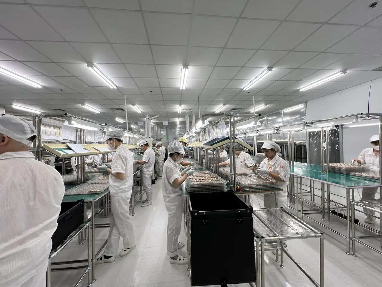
Components located close to V-score lines, tabs, routing paths, or depanelization areas may be exposed to mechanical stress or physical tool interference.
The risk depends on:
- Component package
- Board thickness
- Separation method
- Tab position
- Cutting equipment
- PCB material
- Copper distribution
- Component orientation
- Required edge finish
Extra attention may be required for:
- Multilayer ceramic capacitors
- BGA and QFN packages
- Large inductors or transformers
- Tall connectors
- Heavy components
- Brittle components
- Components with large solder joints
- Parts spanning areas of high board flex
There is no single component-to-edge distance that applies to every design. The final clearance should follow the fabricator’s and assembler’s DFM rules.
The designer should also account for:
- Router-bit diameter
- V-score tolerance
- Tab remnants
- Fixture clearance
- Cutting-head clearance
- Connector overhang
- Operator access
- Inspection-camera visibility
Late discovery of a clearance conflict can require changes to placement, board outline, panel structure, or depanelization method.
Panel Strength and Rigidity
A panel must remain sufficiently stable through printing, placement, reflow, inspection, and handling.
Insufficient rigidity can contribute to:
- Solder-paste misalignment
- Placement errors
- Conveyor jams
- Panel vibration
- Warpage
- Inconsistent support
- AOI focus or image problems
- Premature tab breakage
- Board damage during handling
Panel rigidity is influenced by:
- Overall panel dimensions
- PCB thickness
- Number of routed openings
- Tab quantity and placement
- Rail design
- Copper distribution
- Large internal cutouts
- Board arrangement
- Material type
- Thermal exposure
- Support tooling
A densely routed panel with very narrow tabs may appear acceptable in CAD but become unstable during conveyor transfer.
Balancing strength and easy separation
Increasing tab size can improve rigidity but may increase depanelization force. Reducing tab size can simplify separation but weaken the panel.
The manufacturer must balance:
- Stability during assembly
- Resistance to handling damage
- Tool access
- Acceptable separation stress
- Edge-finish requirements
- Throughput and labor cost
For mechanically sensitive boards, routing or non-contact separation may be preferable to manual breaking.
Panel Warpage
Warpage can interfere with:
- Stencil contact
- Paste transfer
- Component placement
- Reflow support
- Conveyor movement
- AOI imaging
- Fixture contact
Potential contributors include:
- Unbalanced copper
- Large asymmetric openings
- Thin PCB construction
- Uneven board arrangement
- Weak rails
- Inadequate support
- Thermal gradients
- Material characteristics
Panel-level warpage requirements should be confirmed with the assembly equipment capability.
The lists a Yamaha YCP10 printer with a specified panel range of 50 × 50 mm to 460 × 510 mm, panel thickness from 0.4 to 3.0 mm, and panel warp within 2.0 mm. These figures describe listed equipment capability and should not be treated as universal design limits for every product.
Board Orientation Within the Panel
The orientation of individual boards affects material utilization and assembly flow.
Engineers should evaluate:
- Conveyor direction
- Component orientation
- Stencil printing
- Placement-head travel
- Reflow behavior
- AOI accessibility
- Wave or selective soldering
- Connector overhang
- Depanelization sequence
- Operator handling
Rotating alternating boards may improve material utilization, but it can also complicate:
- Placement programming
- Polarity verification
- Visual inspection
- Test fixture design
- Manual assembly
- Traceability
A panel should not be optimized for laminate usage alone. Assembly, test, and separation processes must be considered together.
PCB Panelization for Double-Sided Assembly
Double-sided SMT assembly introduces additional constraints because the panel passes through printing, placement, and reflow more than once.
The panel design should consider:
- Which side is assembled first
- Component weight
- Component retention during second-side reflow
- Support requirements
- Panel flatness
- Conveyor-edge clearance
- Fixture or carrier use
- Reflow profile
- Handling between sides
Tall or heavy components may restrict how the panel is supported during the second pass. Components that extend beyond the finished board outline may interfere with rails or conveyors.
For designs moving from prototype to repeatable production, these factors should be reviewed during NPI in electronics manufacturing, before mass-production tooling is finalized.
Mixed-Design Panelization
Some manufacturers may place different PCB designs on the same fabrication panel. This is sometimes called mixed-panel or family-panel production.
Potential advantages include:
- Producing related boards together
- Reducing setup for low-volume product families
- Coordinating boards used in one final assembly
- Improving material utilization in selected cases
Potential disadvantages include:
- Different component densities
- Different paste requirements
- Different assembly flows
- Different test requirements
- Unbalanced thermal behavior
- Complex traceability
- Difficult replacement if one design has a defect
- Increased programming and material-control risk
For automated assembly, identical multi-up arrays are generally easier to control than panels combining unrelated boards. Mixed designs should be approved by the fabricator and assembler before release.
Depanelization Methods
Depanelization separates finished PCBs from the production panel.
The selected method affects:
- Mechanical stress
- Edge quality
- Throughput
- Labor
- Dust
- Tooling
- Component clearance
- Capital cost
- Dimensional accuracy
Manual breaking
Manual breaking may be used for selected V-scored or mouse-bite panels.
Advantages:
- Minimal equipment
- Simple for low-volume production
- Fast for non-sensitive boards
Risks:
- Inconsistent force
- Board flex
- Component or solder-joint stress
- Operator variability
- Rough edges
- Potential damage near the separation line
Manual breaking is generally unsuitable when the design contains sensitive components close to the board edge.
V-cut depaneling machines
V-cut machines guide and separate boards along pre-scored lines.
They can provide more controlled separation than hand breaking, but the panel remains limited to suitable straight-line geometry.
Router depaneling
Routing uses a mechanical cutting tool to remove tabs or follow the board outline.
Advantages may include:
- Support for complex contours
- Cleaner routed edges
- Controlled separation
- Compatibility with populated panels
Considerations include:
- Tool diameter
- Fixture design
- Cutting dust
- Tool wear
- Mechanical load
- Processing time
- Access around components
Punching
Punching can provide fast separation for high-volume, stable designs. However, it requires dedicated tooling and may apply significant mechanical force.
It is generally less flexible for frequent product changes.
Laser depaneling
Laser depaneling uses a focused beam to separate the PCB without direct mechanical contact.
LPKF describes laser depaneling as a flexible, non-contact process that can reduce mechanical stress compared with conventional separation methods. It is particularly relevant to complex contours, sensitive components, flex circuits, and applications requiring controlled edge quality. (laser depaneling technology)
Laser depaneling may offer:
- Low mechanical stress
- Fine contours
- Small cutting channels
- Reduced tool wear
- Flexible programming
- Clean edge options
It may also involve higher equipment and process costs. The decision should consider product risk, production volume, material, cleanliness requirements, and total cost.
How PCB Panelization Affects Assembly Cost
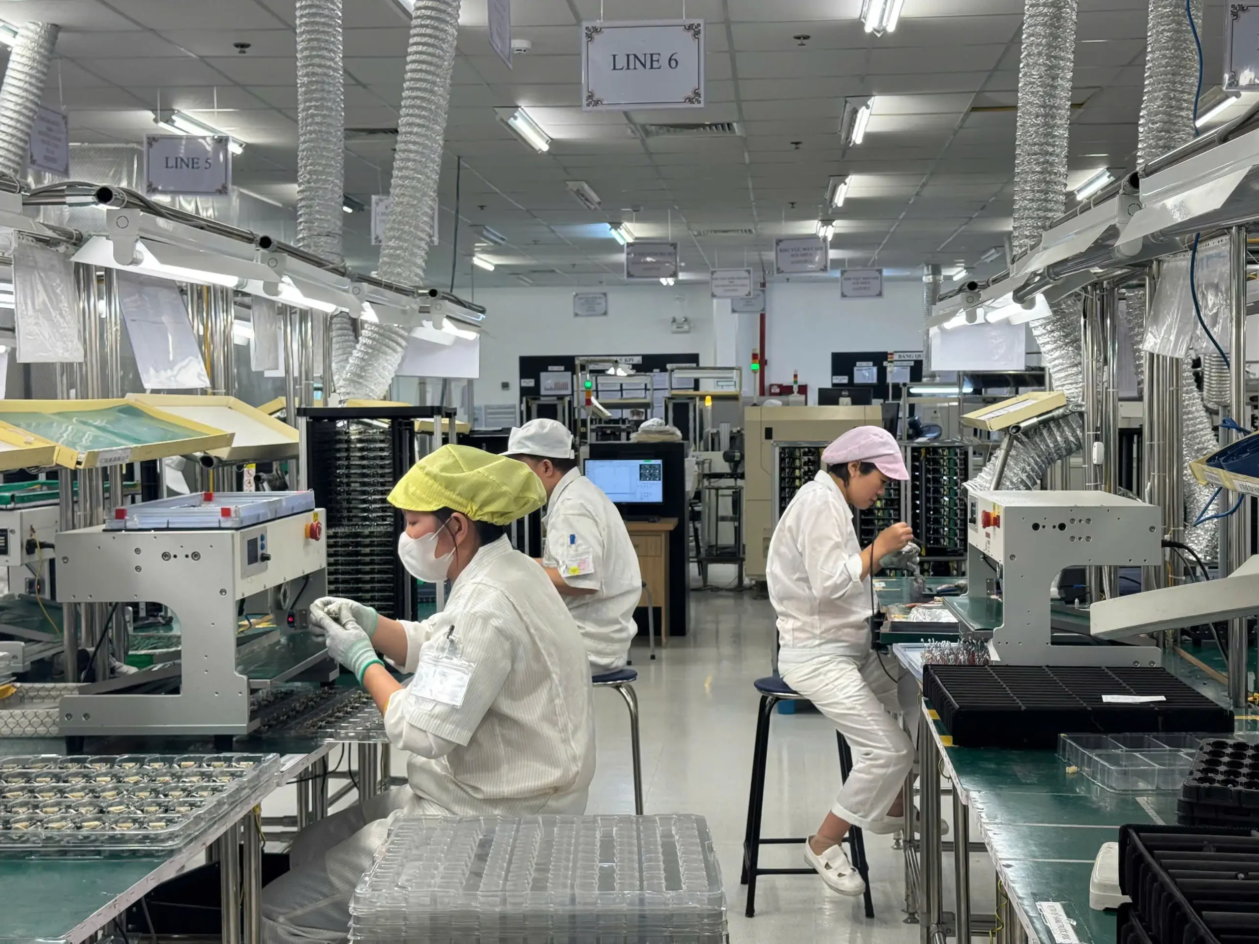
Panelization can reduce or increase manufacturing cost depending on how efficiently it supports the complete process.
Material utilization
More boards per panel can reduce material cost per unit, but overly tight spacing may create weak structures or unsuitable separation paths.
SMT throughput
A multi-up panel can reduce the number of loading, printing, and conveyor cycles per finished PCB.
Machine setup
Standardized panel dimensions may simplify setup, while complex mixed panels may increase programming and verification time.
Routing and depanelization
Tab routing, mouse bites, router separation, and laser cutting introduce different process and tooling costs.
Scrap exposure
A defect affecting one area of a multi-board panel may affect the disposition of several boards. The risk depends on fabrication stage, defect type, repairability, and quality agreement.
Fixtures and carriers
Special carriers may be needed for thin, irregular, or mechanically sensitive panels.
Inspection and testing
Panel-level inspection can improve throughput, but ICT or FCT fixtures may require individual boards to be separated first.
OEMs comparing overall production economics should evaluate panelization alongside the broader PCB assembly cost, rather than focusing only on the number of boards per panel.
Common PCB Panelization Mistakes
| Mistake | Possible impact | Recommended action |
|---|---|---|
| Panel dimensions not confirmed | Incompatibility with SMT equipment | Obtain assembly-house limits before release |
| Missing tooling rails | Poor conveyor handling | Add process rails where required |
| Missing panel fiducials | Alignment problems | Include machine-readable fiducials |
| Weak tab structure | Panel flex or premature breakage | Review rigidity and tab placement |
| Tabs near sensitive components | Depanelization damage | Move tabs or components |
| V-score used on complex geometry | Unmanufacturable separation path | Use routing or another method |
| Connector overhang ignored | Conveyor or fixture collision | Review 3D mechanical clearance |
| No depanelization plan | Late tooling changes | Define method during DFM |
| Mixed orientations without review | Programming and inspection complexity | Standardize orientation where possible |
| Excessive material around boards | Higher cost and waste | Optimize rails and spacing |
| Insufficient edge clearance | Tool or stress interference | Apply manufacturer-specific limits |
| Old panel revision sent | Wrong tooling or array produced | Control panel files and drawings |
The panel design must also match the released PCB assembly quote, because board count per panel, routing, tooling, and depanelization can affect price and lead time.
PCB Panelization Drawing Requirements
The final manufacturing package should include a controlled panel drawing.
The drawing should show:
- Overall panel length and width
- Individual board outlines
- Board-to-board spacing
- Rail dimensions
- V-score lines
- Routed areas
- Tab positions
- Mouse-bite locations
- Tooling holes
- Fiducials
- Panel origin
- Conveyor direction
- Board orientation
- Panel revision
- Depanelization notes
- Finished-edge requirements
The fabrication data and drawing must agree. A line shown as a route in one file and a V-score in another can create serious manufacturing ambiguity.
The complete package should be checked against the PCBA manufacturer Vietnam RFQ checklist before quotation or pilot production.
PCB Panelization Checklist Before Production
Before approving the panel, confirm that:
- The fabricator and assembler have reviewed the design.
- Overall panel dimensions fit the intended equipment.
- Panel thickness and warpage requirements are defined.
- Conveyor direction is identified.
- The selected separation method matches the board geometry.
- V-score lines are straight and clearly documented.
- Routed tabs are positioned away from sensitive components.
- Mouse-bite remnants are acceptable for the enclosure.
- Tooling rails provide adequate handling clearance.
- Global panel fiducials are included where required.
- Local fiducials are evaluated for fine-pitch components.
- Tooling-hole size and position are approved.
- Component-to-edge clearance follows manufacturer rules.
- Connector overhang has been reviewed in 3D.
- Panel rigidity is adequate for printing and placement.
- Double-sided assembly requirements are considered.
- AOI, ICT, and FCT access has been reviewed.
- Depanelization equipment and fixtures are identified.
- Board-edge quality requirements are defined.
- Panel Gerber, drill, route, and drawing revisions match.
- The board quantity per panel matches quotation and planning data.
PCB Panelization for PCBA Manufacturing at SHDC
SHDC’s company profile describes EMS capabilities covering component soldering, assembly, testing, and packaging. Its current factory scope lists four high-speed SMT lines, three DIP lines, one assembly line, one test line, and one packaging line.
The listed production equipment includes:
- Yamaha YSM20R placement equipment supporting PCB sizes from 50 × 50 mm to 810 × 490 mm
- Yamaha YCP10 printing equipment with a listed panel range from 50 × 50 mm to 460 × 510 mm
- Yamaha YSM10 placement equipment supporting PCB sizes from 50 × 50 mm to 510 × 460 mm
- Yamaha 3D SPI
- Yamaha 3D AOI
- Nitrogen reflow
- Wave soldering
- ICT and functional-testing equipment
These machine specifications do not replace a product-specific panel review. SHDC engineering must still assess panel dimensions, rail design, fiducials, warpage, component overhang, double-sided processing, inspection access, and depanelization for each project.
US OEMs evaluating production options can review SHDC’s broader PCBA Vietnam capabilities or its guide to selecting a PCB assembly Vietnam partner.
Conclusion
PCB panelization affects far more than the number of boards placed on one laminate sheet. It influences solder-paste printing, component placement, conveyor handling, reflow stability, inspection, testing, material utilization, and final depanelization.
An effective panel balances production efficiency with rigidity, machine compatibility, component clearance, edge quality, and separation stress. V-scoring may suit straight rectangular arrays, while tab routing supports more complex geometries. Tooling rails, fiducials, tooling holes, board orientation, and depanelization requirements should be approved before the manufacturing package is released.
US OEMs should review panelization jointly with the PCB fabricator and assembly manufacturer during DFM and NPI, rather than allowing panel design to become an uncontrolled manufacturing assumption.
Frequently Asked Questions
What is PCB panelization?
PCB panelization is the process of arranging one or more individual circuit boards into a larger manufacturing panel for fabrication, SMT assembly, inspection, and handling.
Is PCB panelization always required?
No. Large rectangular boards may move through production individually. Small, irregular, fragile, or high-volume boards often benefit from panelization or temporary tooling rails.
What is the difference between V-cut and tab routing?
V-cut uses straight scored grooves that allow rectangular boards to be separated. Tab routing removes most of the outline with a router while leaving selected breakaway tabs, making it more suitable for complex shapes.
What are mouse bites in PCB panelization?
Mouse bites are rows of small perforations used to weaken breakaway tabs. They make manual separation easier but can leave small remnants on the board edge.
Why are tooling rails added to PCB panels?
Tooling rails provide stable conveyor edges and space for fiducials, tooling holes, labels, coupons, and process handling.
What are panel fiducials?
Panel fiducials are optical reference marks placed on the panel or tooling rails. Vision systems use them to align solder-paste printing, component placement, and inspection operations.
How close can components be placed to a V-score?
The required distance depends on the component, PCB material, thickness, depanelization process, and manufacturer rules. Sensitive components should receive additional clearance because board flex can transfer stress into solder joints or component bodies.
Does panelization reduce PCB assembly cost?
It can reduce handling and equipment cycles per board, but rails, routing, fixtures, material waste, and depanelization can add cost. The complete manufacturing process must be evaluated.
Who should create the PCB panel?
The designer, PCB fabricator, or assembly manufacturer may create it. Regardless of ownership, the fabricator and assembler should review and approve the panel before production data is released.
When should panelization be reviewed?
Panelization should be reviewed during DFM and NPI, before the quotation and pilot build are finalized.