Tiếng Việt
 日本語
日本語
An automotive PCB can be electrically correct and still be difficult to manufacture. A board may work during prototype testing but create recurring problems when production volume increases. Pads may not release solder paste consistently. Components may sit too close together for reliable placement or rework. Large copper areas may heat unevenly during reflow. Test points may be inaccessible once the board is installed in a fixture.
These problems are expensive to correct after the stencil, placement program and test fixture have already been completed.
Before PCBA production begins, SHDC reviews the design from an assembly perspective. The objective is not to redesign the customer’s circuit. It is to identify features that could affect solder paste printing, SMT placement, reflow, through-hole assembly, inspection and testing.
SHDC’s documented EMS scope covers component soldering, assembly, testing and final packaging. Its current production infrastructure includes SMT, DIP, AOI, ICT and functional-testing operations.
What Makes an Automotive PCB Different?
There is no single automotive PCB design that applies to every vehicle system. A control board installed in the passenger compartment faces different operating conditions from a module mounted near a motor, pump or exterior sensor.
Depending on the application and customer specification, the design may need to account for:
- Temperature changes
- Mechanical vibration
- Connector and harness loads
- Electrical noise
- Voltage transients
- Moisture or contamination
- Limited enclosure space
- Extended operating life
- Service and diagnostic requirements
These requirements affect more than component selection. They can also influence board thickness, copper distribution, connector mounting, solder-joint geometry, mechanical support and test strategy.
IPC identifies IPC-2221C as the foundation standard in the IPC-2220 printed-board design series. It establishes generic requirements for printed-board design, while more specific product and customer requirements must still be applied to the individual program.
Automotive customers may also maintain their own manufacturing, documentation and approval requirements. The IATF Global Oversight website publishes separate customer-specific requirements for participating OEMs, which means a supplier should not assume that one general automotive control plan will satisfy every customer.
Automotive PCB Design Review at SHDC: Key Areas
Before building a pilot lot, SHDC needs to understand how the board design interacts with the intended production process.
| Review area | What needs to be checked | Why it matters |
|---|---|---|
| Manufacturing files | Gerber, BOM, placement data, drawings and revisions | Prevents mismatched production programs |
| Board format | Dimensions, thickness, warpage and panel design | Determines handling and machine compatibility |
| Footprints | Pad size, pitch, orientation and thermal pads | Affects printing and solder-joint formation |
| Component spacing | Clearance around packages and board edges | Affects placement, AOI, rework and fixtures |
| Thermal design | Copper planes, vias and component mass | Influences the reflow profile |
| Through-hole design | Hole diameter, pads and soldering access | Affects insertion and wave soldering |
| Inspectability | Polarity marks and visible solder features | Supports first-article inspection and AOI |
| Testability | Test points, connectors and programming access | Determines ICT and FCT coverage |
| Special processes | Cleaning, coating, potting or marking | Requires separate process confirmation |
The review typically moves from the design package to DFM and DFT, followed by process planning, pilot production and final manufacturing approval.
1. Start With a Complete Manufacturing Data Package
Gerber files alone are not enough to prepare an automotive PCB for assembly.
They describe the copper, solder mask, legend and other physical layers of the bare board, but they do not give the manufacturer all the information needed to purchase components, program placement machines or build test fixtures.
A complete package should normally contain:
- Gerber or ODB++ data
- PCB fabrication drawing
- BOM with manufacturer part numbers
- Approved component alternatives
- Pick-and-place data
- Assembly drawings
- Schematic
- PCB stack-up
- Surface-finish requirements
- Component datasheets where necessary
- Programming files
- ICT and FCT specifications
- Labeling and packaging instructions
SHDC’s guide to PCB assembly files explains how Gerber, BOM, pick-and-place and assembly drawings work together during production.
Align Every File to the Same Revision
One incorrect revision can invalidate an otherwise complete data package.
Common transfer problems include:
- A BOM containing parts from a newer revision than the Gerber files
- Pick-and-place coordinates exported before the final layout change
- Assembly drawings showing an old polarity direction
- Firmware prepared for a different hardware revision
- Test limits carried over from an earlier product version
The manufacturing package should identify one approved baseline. File names alone are not sufficient; the revision should also appear inside the controlled document or data system.
>>>Read more: Vietnam Automotive Electronics Localization: SHDC’s PCBA Assembly and Testing Capabilities
Identify Critical Components Early
The OEM should clearly identify parts that require additional control, including:
- Polarity-sensitive devices
- Programmed components
- Safety-related parts
- Heat-sensitive components
- Customer-controlled components
- Moisture-sensitive devices
- Parts with approved substitutes
- Components requiring special storage or handling
This information affects material preparation, feeder verification, first-article inspection and testing.
Before requesting a quotation, OEMs can use the PCBA manufacturer Vietnam RFQ checklist to confirm that the technical and commercial package is complete.
2. Review Board Dimensions, Thickness and Panelization
The next question is whether the board or panel can move through the intended printing, placement and soldering route.
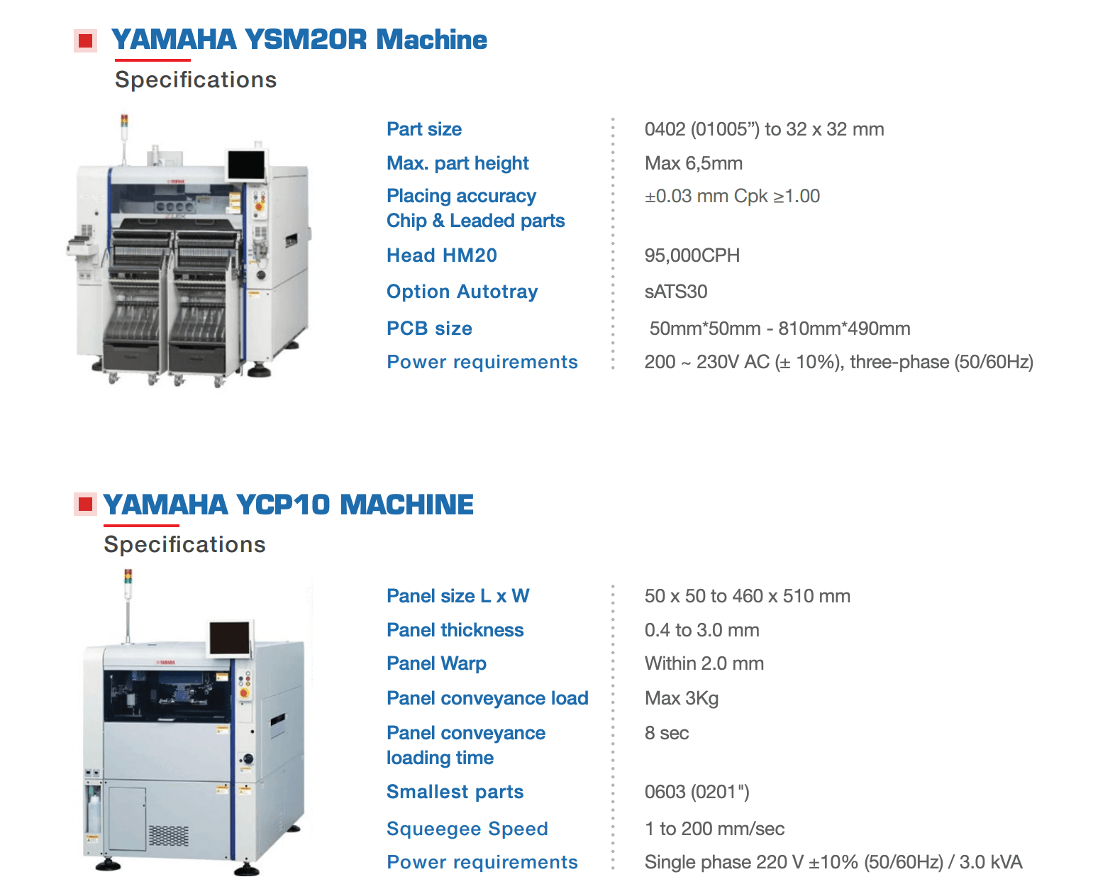
SHDC’s profile lists the following installed-equipment specifications:
- Yamaha YCP10: panel sizes from 50 × 50 mm to 460 × 510 mm and panel thickness from 0.4 to 3.0 mm
- Yamaha YSM20R: PCB sizes from 50 × 50 mm to 810 × 490 mm
- Yamaha YSM10: PCB sizes from 50 × 50 mm to 510 × 460 mm
These values are useful for an initial equipment check, but they are not an automatic manufacturing approval.
A board within the nominal size range may still require changes because of:
- Excessive warpage
- Insufficient edge support
- Component overhang
- Poor panel rigidity
- Conveyor-rail interference
- Unbalanced panel layout
- Incompatible depaneling features
- Tall or heavy bottom-side components
Yamaha’s official YCP10 specifications also show that the printer is designed to support multiple stencil formats and PCB sizes up to 510 × 460 mm, depending on the machine specification. The actual installed configuration and tooling plan should therefore be verified during project review.
Build a Panel for the Process, Not Only for PCB Utilization
A panel that maximizes the number of boards per sheet is not necessarily the best panel for assembly.
SHDC should review:
- Panel rails
- Global and local fiducials
- Tooling holes
- Board orientation
- V-cut or tab-routing method
- Breakaway tabs
- Mouse bites
- Support areas
- Component clearance from the panel edge
The PCB panelization guidelines for assembly provide more detail on V-cuts, tab routing, rails and fiducials.
Consider Depaneling Stress
Components located near a breakaway line can be exposed to mechanical stress when the boards are separated. This is especially relevant for ceramic components, MLCCs and solder joints near the PCB edge.
During the review, the team should consider:
- Distance from sensitive components to the separation line
- Board orientation during depaneling
- Manual versus automated separation
- Support under the PCB
- Potential bending around routed tabs or V-cuts
Moving a component a few millimeters during layout may be simpler than controlling a recurring crack or solder-joint failure during production.
3. Verify Footprints, Pad Geometry and Component Spacing
A footprint must match more than the component’s nominal package name.
The review should compare the land pattern with the actual component drawing, including:
- Pad dimensions
- Lead width and pitch
- Component body size
- Pin-one location
- Exposed thermal pads
- Solder-mask openings
- Courtyard clearance
- Recommended solder pattern
- Package tolerances
A footprint problem may lead to solder bridging, insufficient solder, tombstoning, component rotation or difficult rework.
IPC includes several design standards addressing printed boards, component mounting and assembly considerations. The applicable requirements should be selected based on the board technology, product class and customer specification rather than copied from a generic layout template.
Leave Enough Space for Production
Electrical clearances are only one part of component spacing.
Production clearance may be needed for:
- Placement nozzles
- AOI camera views
- Manual soldering tools
- Rework equipment
- Test probes
- Connector mating
- Heat-sink installation
- Mechanical fasteners
A dense layout may be electrically efficient but difficult to inspect and repair. Tall components can also block the AOI view of smaller parts or solder joints nearby.
Make Polarity Obvious
Polarity and orientation marks should be easy to read both on the drawing and on the physical board.
Useful practices include:
- Clear pin-one indicators
- Consistent diode orientation symbols
- Visible capacitor polarity marks
- Reference designators that remain readable after placement
- Matching orientation between layout, assembly drawing and pick-and-place data
Clear marking reduces dependence on operator interpretation and simplifies AOI-program development.
4. Review the Design for Solder Paste Printing
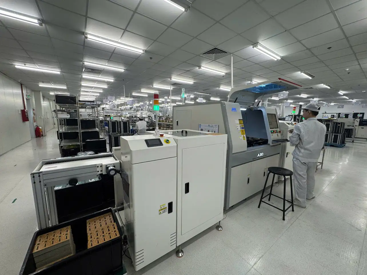
A large share of SMT defects begins at the printing stage.
Stencil design should account for the full component mix rather than applying the same aperture strategy to every pad. SHDC may need to review:
- Stencil thickness
- Aperture reductions
- Fine-pitch components
- Small passive components
- Large exposed pads
- Thermal-pad segmentation
- Mixed pad geometries
- Step-stencil requirements
- Paste-release conditions
A design containing both very small passive components and large power packages may require a compromise between the solder-paste volume needed by each group.
The design for manufacturing guide covers the wider relationship between PCB design decisions and assembly yield.
Design With SPI in Mind
SHDC’s equipment portfolio includes the Yamaha YSi-SP 3D solder paste inspection system. Yamaha lists volume, height, area and misalignment among the system’s inspection items.
SPI is more effective when the board provides:
- Stable support during measurement
- Clearly separated paste deposits
- Controlled board warpage
- Consistent stencil alignment
- Suitable fiducial locations
SPI can identify printing variation before components are mounted, but the inspection limits and sampling or coverage plan still need to be defined for the product.
5. Confirm SMT Placement Compatibility
SHDC’s profile lists Yamaha YSM20R and YSM10 surface-mount machines.
For the installed configurations described in the profile:
- The YSM20R is listed for components from 0402 metric, equivalent to 01005 inch, up to 32 × 32 mm, with a maximum component height of 6.5 mm.
- The YSM10 is listed for components from 03015 up to 55 × 100 mm, with a maximum height of 15 mm.
These figures support an initial package review, but the component body size is not the only consideration.
Placement feasibility can also depend on:
- Feeder type
- Tape, tray or tube packaging
- Nozzle availability
- Component shape
- Center of gravity
- Surface reflectivity
- Package tolerance
- Pickup area
- Placement sequence
- Existing component height
Yamaha’s official YSM10 specifications describe a mounting capability of 46,000 CPH under the manufacturer’s defined optimum conditions. Nominal machine speed should not be used as the expected output for an actual automotive PCB because production throughput also depends on component count, feeder arrangement, inspection, changeover and line balance. (Yamaha Motor Global Site)
Plan the First Article
Before the complete lot is assembled, the first board should be checked for:
- Correct component identity
- Correct polarity
- Package-to-footprint match
- Placement position
- Orientation
- Feeder setup
- Program revision
First-article approval is particularly valuable when similar-looking components have different values or when the same package is used in several locations.
6. Evaluate Thermal Mass and Reflow Requirements
An automotive PCB rarely heats evenly.
Large ground planes, thick copper areas, thermal vias, transformers, shields and large connectors may absorb heat more slowly than small passive components. If the profile is not developed around the actual assembly, some areas may remain too cool while smaller components are exposed to excessive heat.
Potential results include:
- Uneven solder wetting
- Tombstoning
- Cold or incomplete joints
- Component movement
- Flux degradation
- Thermal damage to sensitive parts
SHDC’s profile lists a JT N₂ reflow oven. Nitrogen may support oxidation control when it is appropriate for the solder paste, surface finish and product requirements, but it should not be assumed that every assembly requires or receives a nitrogen process.
The reflow profile should be measured on the actual board or representative panel, with thermocouples placed at relevant thermal locations. Oven-zone settings alone do not show what each component joint experiences.
For projects using lead-free solder, SHDC’s article on lead-free PCB assembly explains alloy selection, thermal profiling and process control in more detail.
7. Design Through-Hole Features for Insertion and Soldering
Many automotive assemblies use a mix of SMT and through-hole components.
Through-hole technology may be chosen for:
- Connectors
- Relays
- Transformers
- Large capacitors
- Power components
- Mechanical switches
- Parts exposed to insertion or harness loads
SHDC currently lists four high-speed SMT lines and three DIP lines. Its profile also shows automatic insertion, AV plug-in equipment, hand insertion, a component-forming machine and JT wave soldering.
For more background on the two assembly methods, see SMT processing vs. through-hole assembly.
Check Hole and Pad Geometry
The review should cover:
- Finished-hole diameter
- Lead diameter and tolerance
- Annular ring
- Lead protrusion
- Component seating
- Hole plating
- Mechanical retention
- Clearance to nearby copper or components
A hole that is too tight can make insertion difficult. A hole that is too large may affect solder fill and mechanical support.
Prepare the Layout for Wave Soldering
Wave-soldering review may include:
- Component orientation relative to solder flow
- Spacing between leads
- Shadowing from large components
- Solder-thieving features
- Bottom-side SMT components
- Pallet requirements
- Board-edge clearance
- Flux and preheat access
Typical risks include insufficient hole fill, solder bridges, solder skips, icicles and non-wetting. SHDC’s guide to common PCB assembly defects explains how design and process conditions contribute to these failures.
8. Make the Board Inspectable
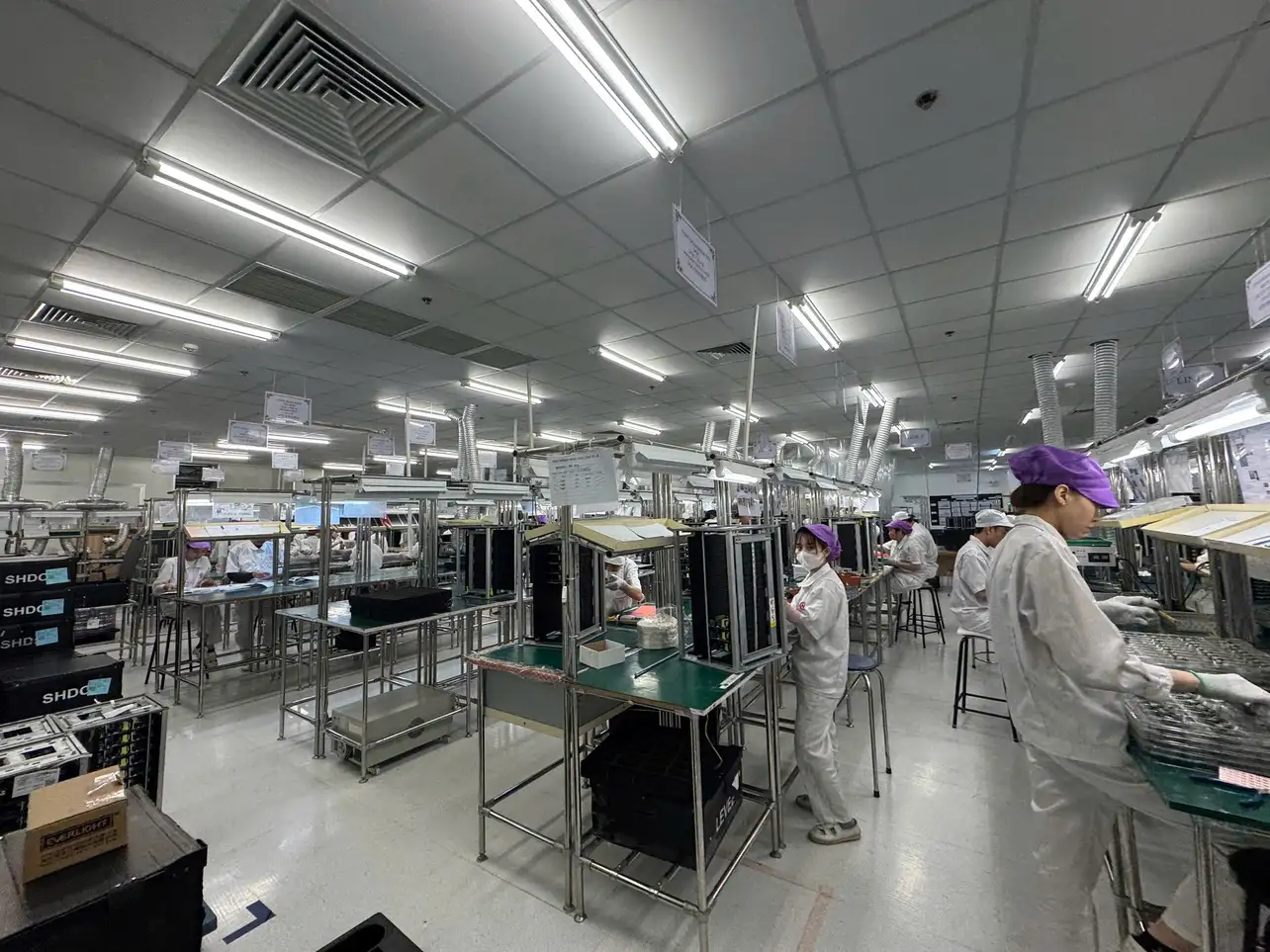
Inspection should be considered during layout, not after the first defective lot.
A board designed for AOI should provide reasonable visibility of:
- Component edges
- Polarity marks
- Lead positions
- Visible solder fillets
- Reference markings
- Small components near taller packages
SHDC’s equipment portfolio lists the Yamaha YSi-V 3D AOI. Yamaha describes the system as combining 2D inspection, 3D inspection and four-direction oblique imaging, with inspection targets covering mounted components and visible post-soldering conditions.
The internal guide to automated optical inspection in PCB assembly provides a fuller explanation of AOI programming and defect review.
Understand What AOI Cannot Prove
AOI does not automatically verify:
- Component electrical value
- Firmware
- Communication functions
- Internal BGA joints
- Hidden solder conditions
- Complete circuit behavior
- Long-term reliability
A board containing BGA, bottom-termination or other hidden-joint packages may require an additional inspection plan. SHDC’s available profile does not confirm in-house X-ray inspection, so this requirement should be discussed before the quotation and pilot build.
9. Add Testability Before the Layout Is Released
Test coverage is strongly influenced by PCB design.
If the test points are added after routing is complete, there may be no practical space for probes, fixture support or programming access.
The design for testability guide explains how product design decisions affect production testing.
ICT Access
SHDC’s profile lists the Kyoritsu ICT F-2000 Plus. Depending on the fixture and test program, ICT may be used to evaluate opens, shorts, continuity and selected component-level conditions.
The PCB review should consider access to:
- Power rails
- Ground
- Critical signals
- Analog measurement points
- Programming lines
- Communication buses
- Diagnostic nodes
- Safety-related nets
Fixture access also depends on:
- Test-point diameter
- Probe spacing
- Tall-component clearance
- Board support
- Alignment holes
- Connector position
- Single- or double-sided probing
No fault-coverage percentage should be assumed before the netlist, fixture strategy and available test access have been reviewed.
Functional-Test Access
FCT normally requires more than exposed pads.
The OEM may need to define:
- Power input
- Connector pinout
- Programming interface
- Communication interface
- Input stimuli
- Simulated loads
- Expected outputs
- Timing limits
- Firmware revision
- Pass/fail criteria
SHDC’s comparison of ICT vs. functional testing explains why the two methods address different failure types.
CAN, LIN, automotive Ethernet or other product-specific interfaces should not be assumed from the presence of general functional-test equipment. Each interface requires an approved fixture, instrumentation and test specification.
10. Define Cleaning, Coating and Post-Assembly Requirements
Post-assembly requirements can change the PCB layout.
For example, cleaning requirements may affect:
- Flux selection
- Sensitive components
- Trapped residue under low-clearance parts
- Areas that cannot be washed
- Ionic-cleanliness acceptance
Conformal coating may require:
- Keep-out zones
- Masking around connectors
- Accessible test points
- Clearance around heat sinks
- Protected grounding contacts
- Defined coating thickness
- Cure and inspection requirements
The current SHDC profile does not confirm an in-house conformal-coating line, selective-coating equipment, UV inspection, parylene coating or potting capability. These processes should therefore be treated as project-specific requirements that need separate confirmation.
The profile does show backend assembly and laser-marking equipment. When these processes are required, the OEM should provide marking content, barcode or serial format, location, mechanical drawings and assembly instructions.
11. Validate the Design Through a Pilot Build
A DFM report can identify likely risks, but the pilot build shows how the design performs on the actual production route.
The pilot should confirm:
- File and revision accuracy
- Panel handling
- Stencil performance
- SPI results
- Placement setup
- Reflow profile
- AOI programming
- Through-hole insertion
- Wave-soldering quality
- ICT fixture operation
- FCT sequence
- Packaging
The team should also review early production data, including:
- Printing defects
- Placement errors
- Reflow defects
- AOI false calls
- Through-hole soldering issues
- ICT failures
- Functional failures
- First-pass yield
- Rework rate
Results may lead to changes in the stencil, footprint, component spacing, panel rails, polarity marking, test-point location or fixture support.
After approval, the baseline should control the PCB revision, BOM, stencil, machine programs, inspection programs, test software, firmware, work instructions and packaging requirements.
SHDC Capabilities: Confirmed and Project-Specific
SHDC’s current profile documents approximately 2,600 square meters of factory area, 150 employees, four high-speed SMT lines, three DIP lines, one assembly line, one test line and one packaging line.
| Area | Shown in SHDC’s profile | What still needs project review |
|---|---|---|
| Solder paste printing | Yamaha YCP10 | Panel, stencil and support compatibility |
| SPI | Yamaha YSi-SP 3D SPI | Inspection limits and production coverage |
| SMT placement | Yamaha YSM20R and YSM10 | Package, feeder and nozzle compatibility |
| Reflow | JT N₂ reflow oven | Product-specific thermal profile |
| AOI | Yamaha YSi-V 3D AOI | Program scope and defect criteria |
| DIP assembly | Three DIP lines and insertion equipment | Component and tooling route |
| Wave soldering | JT wave-soldering equipment | Orientation, pallet and process settings |
| ICT | Kyoritsu ICT F-2000 Plus | Fixture, access and fault coverage |
| Functional testing | Equipment shown in profile | Product-specific interface and program |
| Additional testing | High-voltage, A/V and aging equipment | Applicability to the specific assembly |
| X-ray inspection | Not confirmed | Hidden-joint inspection route |
| Conformal coating | Not confirmed | Availability or outsourced process |
| Automotive certification | Not confirmed in the available profile | Current certificate, site and scope |
The profile separately describes a Phase 2 factory planned for March 2027. Its proposed lines, output and headcount are future targets and should not be presented as current production capacity.
Automotive PCB Design Review Checklist
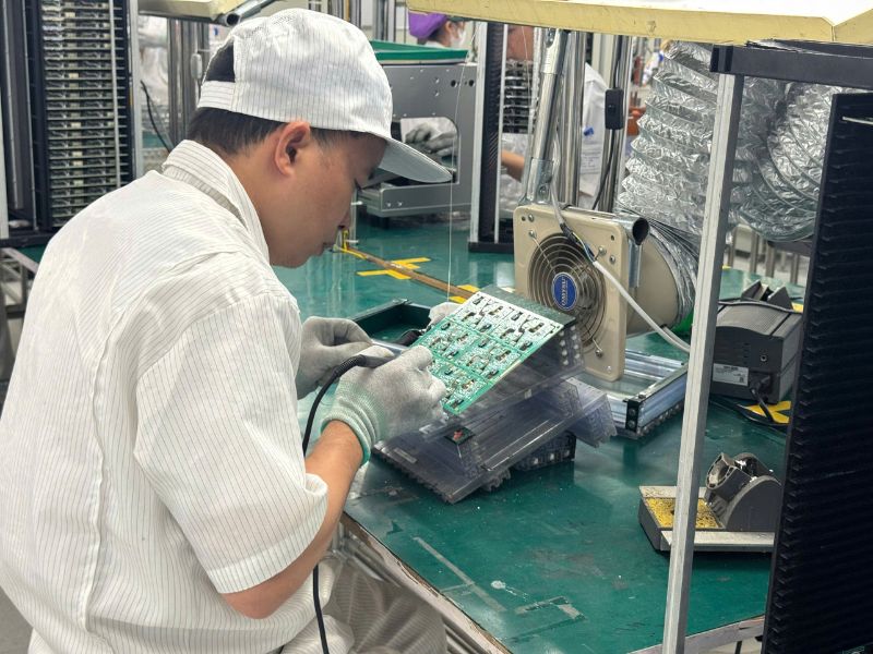
Before releasing an automotive PCB for pilot production, verify that:
- PCB, BOM and assembly files use the same revision.
- Board dimensions and thickness fit the intended process.
- Panel rails, tooling holes and fiducials are defined.
- Component footprints match approved package drawings.
- Pin-one and polarity marks are visible.
- Component spacing supports placement, inspection and rework.
- Stencil apertures are reviewed for the complete package mix.
- Thermal mass and copper distribution are considered.
- Temperature-sensitive components are identified.
- Through-hole pads and finished holes are correctly sized.
- Wave-soldering clearance is available.
- ICT test points are accessible.
- Programming and FCT interfaces are defined.
- Hidden joints have an approved inspection method.
- Cleaning, coating and potting requirements are documented.
- Pilot-build acceptance criteria are agreed.
- Rework and retest requirements are controlled.
- Engineering changes require formal approval.
Conclusion: Review the PCB Before Building the PCBA
A successful automotive PCB is not only electrically correct. It must also move through printing, placement, soldering, inspection and testing without introducing avoidable variation.
Board dimensions, panelization, footprints, component spacing, copper distribution, polarity markings and test access all influence production performance. Reviewing these features early gives the OEM and SHDC time to correct problems before money is committed to stencils, fixtures and volume materials.
SHDC’s documented SMT, DIP, AOI, ICT and functional-testing infrastructure provides a foundation for automotive PCBA evaluation. However, machine specifications are only the starting point. Final manufacturability must be confirmed against the real design, component package, process route and customer requirements.
A structured automotive PCB review helps SHDC identify assembly and testing risks before they become recurring production defects.
Frequently Asked Questions
What is automotive PCB design for assembly?
It is the practice of designing a printed circuit board so that it can be printed, populated, soldered, inspected, tested and repaired consistently during production.
Does SHDC manufacture bare automotive PCBs?
SHDC’s available company profile focuses on EMS and PCBA operations, including component soldering, assembly, testing and packaging. Bare PCB fabrication should be confirmed separately.
What files does SHDC need for a DFM review?
The typical package includes Gerber or ODB++, fabrication drawings, BOM, pick-and-place data, assembly drawings, schematic, component information and test requirements.
Why are fiducials important?
Fiducials give printing, placement and inspection equipment reference points for determining the position and orientation of the PCB or production panel.
Why does component spacing matter?
Spacing affects placement-nozzle access, soldering, AOI visibility, manual rework, connector installation and test-fixture access.
Can SHDC assemble both SMT and through-hole components?
Yes. SHDC’s current profile lists four high-speed SMT lines and three DIP lines. The exact product fit and assembly route still require an engineering review.
Does every automotive PCB need ICT and FCT?
No. The test route depends on product risk, production volume, available test access and customer requirements.
Can AOI inspect every solder joint?
No. AOI is limited when joints are hidden beneath packages such as BGAs or bottom-termination components. Additional inspection methods may be required.
When should DFM and DFT reviews be completed?
They should be completed before the layout is frozen, stencil and fixture tooling are ordered, and pilot production begins.
>>>Read more: Automotive PCBA Vietnam | Trusted Non-China Manufacturer for USA