
 Tiếng Việt
 日本語
日本語
A failed printed circuit board assembly does not automatically reveal why it failed. A product that will not power on may have a damaged component, an open solder joint, incorrect firmware, an unstable power rail, a test-fixture problem, or a defect introduced during handling. Effective PCBA failure analysis is a structured investigation used to move from a reported symptom to a verified root cause. It combines failure reproduction, production-history review, visual inspection, electrical troubleshooting, nondestructive analysis, destructive analysis where necessary, and controlled verification.
For US OEMs, the quality of the investigation matters as much as the speed of the response. Replacing a component may restore one board, but it does not prove why the failure occurred or whether other units are at risk.
A complete investigation should answer five questions:
- What failed?
- How did it fail?
- Why did it fail?
- Which products or lots may be affected?
- What action will prevent recurrence?
What Is PCBA Failure Analysis?
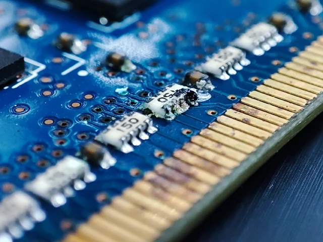
PCBA failure analysis is the systematic process of identifying the physical, electrical, material, design, manufacturing, or operational cause of a circuit-board assembly failure.
The process normally includes:
- Confirming the reported failure
- Preserving the original sample condition
- Collecting product and production records
- Reproducing the symptom
- Localizing the faulty circuit or component
- Identifying the failure mechanism
- Developing possible root-cause hypotheses
- Testing those hypotheses
- Defining containment and corrective action
- Verifying that the action is effective
A structured investigation may use bench electrical testing, visual inspection, X-ray, computed tomography, cross-section analysis, microscopy, material analysis, and manufacturing-data review. An IPC technical paper on a structured approach to failure analysis and root-cause determination demonstrates how several methods can be combined to narrow a complex PCB problem to a defensible cause.
Failure analysis is different from routine production inspection. Inspection determines whether a unit meets defined acceptance criteria. Failure analysis investigates why a unit did not meet those criteria or stopped performing as intended.
Failure Symptom, Defect, Failure Mechanism and Root Cause
A strong report must distinguish between the observed symptom and the underlying cause.
| Term | Meaning | Example |
|---|---|---|
| Failure symptom | What the user or test system observes | The product does not power on |
| Defect | The physical or electrical nonconformity found | An open solder joint is present |
| Failure mechanism | The process through which performance was lost | A solder crack created an intermittent connection |
| Root cause | The underlying condition that produced the mechanism | Excessive board flex during depanelization damaged the joint |
| Contributing factor | A condition that increased the likelihood or severity | The component was located close to the panel breakaway tab |
Finding a cracked solder joint is not always the end of the investigation. The crack may have resulted from:
- Inadequate solder formation
- Thermal cycling
- Mechanical shock
- PCB bending
- Component-package interaction
- Poor pad design
- Rework damage
- Inappropriate depanelization
- Excessive operating temperature
The investigation should continue until the evidence explains both the physical defect and the conditions that created it.
When Is PCBA Failure Analysis Required?
Formal analysis may be needed when:
- A first article does not meet requirements
- Production yield falls unexpectedly
- ICT or functional failures repeat at the same circuit location
- An intermittent problem cannot be reproduced consistently
- A customer returns a failed unit
- Several failures occur within the same production lot
- A product fails under temperature, vibration, humidity, or electrical load
- A previously stable product develops a new failure pattern
- A component supplier, process, design, or firmware revision changes
- The potential consequence of failure is significant
Not every isolated production defect requires a laboratory-level investigation. However, repeated, safety-related, field, or unexplained failures generally require a documented process beyond routine repair.
A review of the existing PCBA testing process is often the first step because test coverage, fixture condition, test limits, and historical results can help determine whether the problem originated in the product or in the verification system.
>>>Read more: PCB Panelization Guidelines for Assembly: V-Cut, Tab Routing, Rails and Fiducials
The PCBA Failure Analysis Process
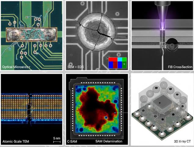
The exact sequence depends on the failure, but a disciplined investigation usually follows the stages below.
Step 1: Preserve the Sample and Collect Failure Information
The failed board should be preserved before anyone cleans, repairs, reflows, or replaces components.
Early handling can destroy evidence such as:
- Flux or contamination residue
- Burn marks
- Corrosion
- Cracked solder
- Foreign material
- Loose hardware
- Connector damage
- Intermittent contact
- Signs of previous rework
Photograph both sides of the assembly and any relevant connectors, cables, enclosures, labels, or damage. Record who received the sample, when it arrived, and what actions were performed.
Product identification
Collect:
- Product name and model
- PCB part number
- Assembly revision
- Serial number
- Production date
- Production lot
- Bare PCB lot
- Component lots where available
- Firmware version
- Test-program revision
- Rework history
Failure information
Document:
- Reported symptom
- Operating condition
- Failure frequency
- Whether the failure is permanent or intermittent
- Environmental conditions
- Applied input and load
- Time in service
- Customer troubleshooting already performed
- Whether the board was dropped, exposed to moisture, or modified
- Whether the failure changes with temperature, pressure, movement, or time
The initial problem statement should describe observable behavior rather than assume a cause.
For example:
“The output voltage falls below the specified limit after 20 minutes at rated load.”
This is more useful than:
“The power component is defective.”
The second statement introduces an unverified conclusion before testing begins.
Step 2: Verify and Reproduce the Failure
A reported failure must be confirmed under controlled conditions.
The investigation should determine:
- Whether the symptom can be reproduced
- Which inputs or operating modes trigger it
- How long it takes to appear
- Whether the failure is temperature-dependent
- Whether movement or vibration changes the result
- Whether the condition disappears after a power cycle
- Whether firmware or configuration affects it
Verify the test system first
Before concluding that the PCBA is defective, check:
- Power supply
- Test fixture
- Probes and connectors
- Cables
- Software
- Test-program revision
- Calibration status
- Limit settings
- Golden sample
- Operator setup
A worn fixture contact or incorrect program limit can create a false production failure.
The difference between electrical verification methods is explained further in ICT versus functional testing.
Compare a failed board with a known-good board
A good-board comparison can reveal:
- Different current consumption
- Missing power rails
- Abnormal waveforms
- Temperature differences
- Incorrect resistance
- Unexpected firmware behavior
- Component-marking differences
- Variation in startup sequence
The comparison board must be the same approved design and configuration. Comparing different revisions may introduce misleading differences.
Step 3: Conduct Visual and Microscopic Inspection
Visual inspection is usually one of the first nondestructive steps.
Inspect the board under suitable lighting and magnification for:
- Missing or shifted components
- Incorrect polarity
- Solder bridges
- Insufficient solder
- Cracked joints
- Lifted leads
- Lifted pads
- Damaged traces
- Burned areas
- Corrosion
- Contamination
- Bent connector pins
- Foreign objects
- Mechanical impact
- Previous rework
- Damaged coatings or labels
A detailed understanding of visible production issues can be supported by reviewing common PCB assembly defects and common SMT and wave-soldering defects.
Inspect the entire assembly
The obvious damaged area may not be the origin of the failure.
For example:
- A burned component may be the result of an upstream overvoltage.
- A blown fuse may have protected the circuit from another short.
- A cracked connector may have been caused by enclosure misalignment.
- Corrosion may extend beyond the visibly affected area.
Inspection should include mechanical interfaces, cables, mounting points, heat sinks, shields, fasteners, and any enclosure features that can apply stress to the PCB.
Step 4: Perform Electrical Troubleshooting
Electrical troubleshooting narrows the failure from a system symptom to a circuit, net, component, or interface.
Common checks include:
- Continuity
- Resistance to ground
- Power-rail voltage
- Current consumption
- Leakage current
- Signal waveforms
- Clock presence
- Reset behavior
- Communication activity
- Component input and output
- Short-circuit localization
Use the schematic and expected sequence
The engineer should understand:
- How power enters the board
- Which rails start first
- Which enable signals are required
- How reset is released
- Which communication paths are active
- What feedback controls the circuit
- What expected values should appear at each stage
Replacing components randomly can introduce new damage without identifying the faulty circuit.
Use controlled isolation
Useful methods may include:
- Disconnecting loads
- Isolating circuit branches
- Comparing resistance with a good board
- Injecting a controlled voltage
- Monitoring thermal response
- Swapping a socketed or removable module
- Replacing a suspected component only after documenting evidence
Component replacement may support a hypothesis, but it is not sufficient by itself to establish root cause.
If replacing one integrated circuit restores function, the investigation must still determine whether the component failed because of:
- An internal device defect
- Electrical overstress
- Excess temperature
- Incorrect surrounding components
- Poor soldering
- Handling damage
- Firmware behavior
- An external load
Step 5: Use AOI, X-Ray and Advanced Analysis Where Appropriate
The selected method should match the suspected failure mechanism.
Automated Optical Inspection
Historical AOI images and results may help determine whether a visible defect was present at production.
AOI may provide evidence for:
- Missing components
- Wrong components
- Polarity errors
- Placement shift
- Visible solder bridges
- Some solder-joint abnormalities
However, a current AOI inspection cannot always prove when a defect occurred. Review machine records, program revision, verification results, and repair history where available.
More information is available in SHDC’s guide to Automated Optical Inspection in PCB assembly.
X-ray inspection
X-ray can reveal conditions that are hidden beneath components, including:
- BGA solder connections
- QFN and bottom-terminated joints
- Voids
- Bridges
- Missing solder
- Solder-ball alignment
- Some internal cracks
- Connector or package features not visible optically
Standard two-dimensional X-ray may not reveal every crack orientation. CT or other methods may be required when the suspected feature overlaps with surrounding structures.
Cross-section analysis
Cross-sectioning can expose:
- Solder-joint structure
- Intermetallic layers
- Cracks
- Voids
- Pad separation
- Plated-through-hole conditions
- Via defects
- Delamination
- Internal laminate damage
Because cross-sectioning destroys the sample, it should be planned after nondestructive evidence has identified the correct location.
Dye-and-pry testing
Dye-and-pry analysis may be useful for identifying cracks beneath BGA or similar packages. Dye penetrates existing fractures before the package is mechanically separated, helping show where joints were cracked before removal.
The process is destructive and requires careful interpretation. Damage created during package removal must not be mistaken for the original failure.
Material and contamination analysis
Depending on the hypothesis, testing may include:
- Ionic contamination analysis
- Fourier-transform infrared spectroscopy
- Scanning electron microscopy
- Energy-dispersive X-ray spectroscopy
- Metallographic analysis
- Surface-residue analysis
- Component decapsulation
IPC test methods provide defined procedures for evaluating specific printed-board failure mechanisms. For example, an IPC-TM-650 test method for conductive anodic filament growth addresses electrochemical migration risks associated with materials, design, and manufacturing conditions.
Not every supplier maintains every advanced analytical capability internally. Complex analysis may require an independent laboratory with appropriate equipment and expertise.
Step 6: Identify the Failure Mechanism

The failure mechanism describes the physical or electrical process through which the assembly lost functionality.
Common PCBA failure mechanisms include:
- Open circuit
- Short circuit
- Intermittent connection
- Solder fatigue
- Brittle solder fracture
- Pad cratering
- Plated-through-hole cracking
- Via failure
- Delamination
- Corrosion
- Electrochemical migration
- Electrical overstress
- Electrostatic discharge
- Thermal damage
- Mechanical cracking
- Component degradation
- Insulation breakdown
- Connector wear
- Firmware corruption
The same symptom may result from different mechanisms.
For example, intermittent communication may be caused by:
- A cracked solder joint
- A marginal connector
- A damaged cable
- A power-rail disturbance
- Clock instability
- Firmware timing
- Electromagnetic interference
The investigation should select the mechanism supported by physical and electrical evidence.
Step 7: Determine the Root Cause
After identifying the mechanism, determine why it occurred.
Root-cause analysis may include:
- 5 Why analysis
- Fishbone diagram
- Fault-tree analysis
- Process-data review
- Design review
- Material-lot comparison
- Good-versus-failed sample comparison
- Timeline analysis
- Controlled experiments
- Statistical analysis
- Supplier investigation
Review the complete production history
Potential evidence includes:
- Incoming inspection results
- Solder-paste lot
- SPI data
- Placement records
- Reflow profile
- AOI results
- ICT and FCT results
- Repair records
- Operator and line
- Machine-program revision
- Equipment maintenance
- Approved deviations
- Engineering changes
A board may have passed production testing but failed later because the test did not expose the relevant condition. This is why design for testability should be considered during development rather than after failures begin.
Consider design, process and use conditions together
Root causes may originate from:
- Circuit design
- PCB layout
- Footprint design
- Material selection
- Component quality
- Soldering process
- Assembly handling
- Rework
- Mechanical integration
- Test coverage
- Packaging
- Transportation
- Customer use
- Environmental exposure
Avoid assuming the cause belongs to the department that first detected the issue.
Step 8: Verify the Root Cause
A root cause should be demonstrated, not merely described.
Verification methods may include:
- Reproducing the failure under the suspected condition
- Removing the suspected condition and confirming the failure disappears
- Repeating the experiment across multiple samples
- Comparing affected and unaffected production lots
- Rebuilding boards using the corrected process
- Testing an updated design
- Reviewing performance after corrective action
- Conducting environmental or accelerated testing where appropriate
For solder-joint fatigue, IPC-9701B defines a thermal-cycling method used to characterize surface-mount solder-attachment fatigue life. Such qualification testing is different from routine troubleshooting, but it may help validate a design or process correction when thermal-mechanical reliability is involved.
Example of root-cause verification
Suppose returned products contain cracked ceramic capacitors close to the PCB edge.
An initial hypothesis may be excessive bending during depanelization.
Verification could include:
- Documenting crack location and orientation.
- Comparing failures with tab or V-score positions.
- Measuring board strain during the current separation process.
- Separating new samples using the existing method.
- Inspecting the capacitors.
- Moving the tab, changing the tool, or increasing component clearance.
- Repeating the experiment.
- Confirming the crack no longer occurs under the revised condition.
This evidence is stronger than stating, “The capacitor was damaged during production.”
Determine the Affected Scope Through Traceability
Failure analysis must identify which other units may share the same risk.
Relevant traceability data may include:
- Product serial number
- PCB lot
- Component lot and date code
- Material supplier
- Production date
- SMT line
- Machine program
- Reflow profile
- Test program
- Firmware version
- Rework history
- Shipment lot
IPC-1782B establishes risk-based minimum requirements for manufacturing and supply-chain traceability for electronic products. The appropriate traceability level should be agreed between the user and supplier according to product risk.
A detailed discussion is available in SHDC’s guide to traceability in electronics manufacturing.
Traceability helps the team avoid two opposite errors:
- Containing too few products and allowing additional failures to escape.
- Containing every product unnecessarily when only one material or process lot was affected.
Containment, Correction and CAPA
These actions should not be treated as interchangeable.
| Action | Purpose | Example |
|---|---|---|
| Containment | Protect customers while investigation continues | Hold the affected lot and inspect warehouse stock |
| Correction | Address the current nonconforming unit | Replace the cracked connector |
| Corrective action | Eliminate the verified cause | Redesign the fixture that applies excessive force |
| Systemic preventive action | Apply lessons to related risks | Review similar fixtures and products |
| Effectiveness validation | Confirm the action works over time | Monitor subsequent lots and confirm no recurrence |
Immediate containment
Containment may include:
- Stopping shipment
- Holding work in process
- Identifying affected serial numbers
- Inspecting warehouse inventory
- Sorting a production lot
- Notifying the OEM
- Reviewing units already shipped
- Implementing temporary additional testing
Containment should begin before the investigation is complete when customer risk justifies action.
Corrective action
Corrective action may involve:
- Updating a process parameter
- Changing tooling
- Improving a work instruction
- Revising a PCB layout
- Changing an approved material
- Adding a test point
- Updating the test program
- Revising the control plan
- Retraining personnel
- Strengthening incoming inspection
- Improving supplier controls
Changes to released design or manufacturing documentation should follow a controlled Engineering Change Order process.
Effectiveness validation
Do not close CAPA immediately after implementation.
Effectiveness should be evaluated through:
- Subsequent production lots
- Yield and defect trends
- Repeat testing
- Customer-return data
- Process audits
- Reliability testing
- Verification that revised documents are in use
- Confirmation that the problem has not moved elsewhere
A corrective action is not effective simply because the first rebuilt board passes.
What Should a PCBA Failure Analysis Report Include?
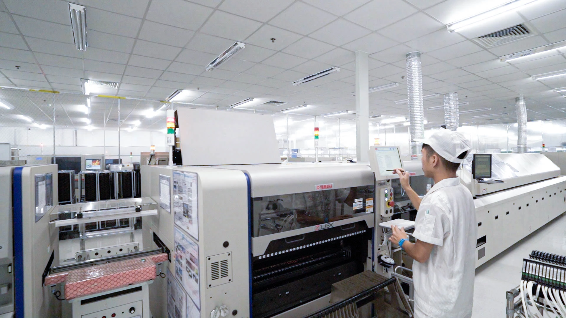
A customer-facing report should make the evidence and reasoning easy to follow.
1. Product identification
Include:
- Product and part number
- Revision
- Serial number
- Production lot
- Firmware
- Sample quantity
- Receipt date
2. Failure description
State:
- Reported symptom
- Verification result
- Test conditions
- Failure frequency
- Environmental conditions
- Pass/fail criteria
3. Sample condition
Document:
- Physical condition on receipt
- Packaging
- Signs of rework
- Damage
- Contamination
- Missing parts
- Photographs
4. Investigation methods
List:
- Visual inspection
- Microscopy
- Electrical measurements
- AOI review
- X-ray
- Cross-section
- Material analysis
- Environmental testing
- Production-record review
5. Findings and evidence
Present:
- Measurements
- Images
- Waveforms
- Test data
- Lot comparison
- Process records
- Physical-analysis results
Clearly separate observations from interpretations.
6. Failure mechanism
Explain how the identified defect caused the reported symptom.
7. Root cause
State the verified underlying cause and supporting evidence.
8. Affected scope
Define:
- Affected lots
- Potentially affected serial numbers
- Inventory status
- Shipped quantity
- Basis for the containment boundary
9. Containment and corrective action
List:
- Immediate controls
- Permanent actions
- Responsible owner
- Due date
- Document revisions
- Customer approvals required
10. Effectiveness validation
Define:
- Validation method
- Sample size or production period
- Acceptance criteria
- Results
- CAPA closure decision
Common PCBA Failure Analysis Mistakes
Confusing a symptom with a root cause
“Product does not start” is a symptom, not a cause.
Replacing a component and ending the investigation
A failed component may have been damaged by another condition.
Altering the sample before documenting it
Cleaning, reflowing, probing, or removing parts may destroy evidence.
Failing to check the test equipment
A fixture, program, or cable may create false failures.
Comparing different product revisions
The observed differences may be intentional design changes.
Selecting a favorite hypothesis too early
Investigators may search only for evidence that supports their first assumption.
Using destructive analysis too soon
Cross-sectioning the wrong location can destroy the only available sample without finding the defect.
Ignoring production and traceability records
Physical analysis alone may not reveal when or where the problem was introduced.
Failing to verify root cause
A plausible explanation is not the same as demonstrated causation.
Closing CAPA before validating effectiveness
The problem may return in later lots.
PCBA Failure Analysis Checklist for US OEMs
When reviewing a supplier report, ask:
- Was the original symptom reproduced?
- Was the test equipment verified?
- Was the failed sample preserved?
- Was a known-good board used for comparison?
- Are observations separated from assumptions?
- Was the failure mechanism identified?
- Does the evidence support the claimed root cause?
- Was the affected production scope defined?
- Which lots and serial numbers were contained?
- Were material and production records reviewed?
- Was the hypothesis experimentally verified?
- Does the corrective action eliminate the cause or only repair the board?
- Were relevant procedures, control plans, or drawings updated?
- Was customer approval obtained for product changes?
- How will effectiveness be monitored?
- What evidence is required before CAPA closure?
US OEMs evaluating a new supplier should also review its diagnostic, testing, traceability, and corrective-action capabilities during supplier qualification. SHDC’s PCB Assembly Vietnam guide provides additional questions to consider before sending an RFQ.
How Better Design and Production Planning Reduce Failure-Analysis Risk
Failure analysis is necessary when problems occur, but early planning can make failures easier to detect, isolate, and prevent.
Useful practices include:
- Accessible test points
- Clear power-domain separation
- Diagnostic firmware
- Controlled production files
- Traceable component lots
- Defined test limits
- Stored test data
- First article approval
- Production validation
- Documented change control
The purpose of Production Validation Testing is to confirm that the product and manufacturing process can meet requirements before full production scale-up.
Likewise, reviewing the full PCBA manufacturing process helps OEM teams identify where quality records should be created and retained for future investigation.
PCBA Failure Investigation Support at SHDC
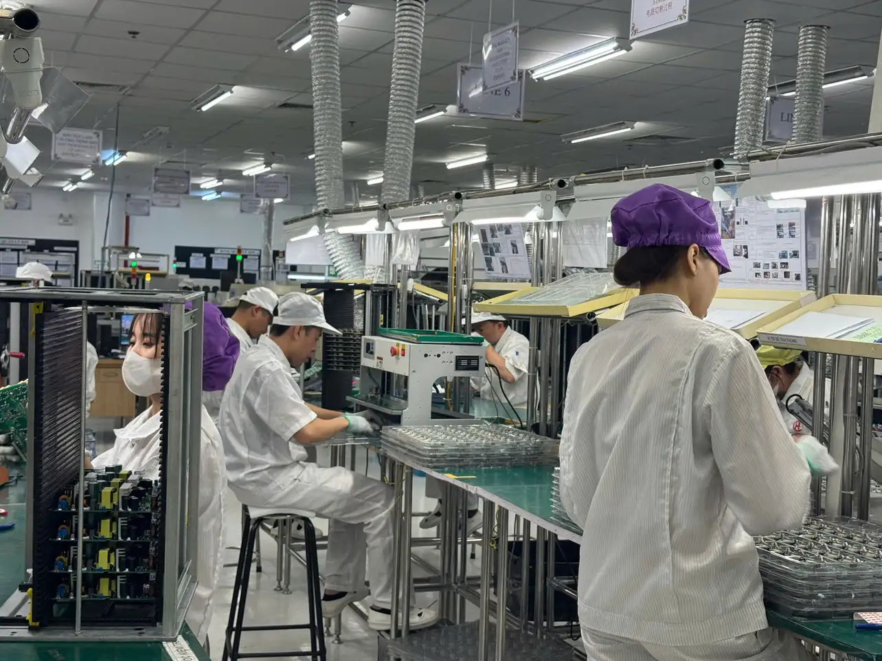
SHDC provides EMS activities from component soldering and assembly through testing and final packaging. Its current factory scope lists four high-speed SMT lines, three DIP lines, one assembly line, one test line, and one packaging line.
The documented production flow includes IQC, screen printing, component placement, reflow, AOI, repair, ICT, visual inspection, FCT, OQC, and packaging. Listed production equipment includes 3D SPI, 3D AOI, ICT, wave soldering, nitrogen reflow, and functional-testing equipment.
These production checkpoints can provide important first-line evidence for a failure investigation, including inspection results, electrical-test outcomes, process history, and repair status. Advanced methods such as CT, SEM, cross-sectioning, or specialized material analysis may require appropriate external laboratory support depending on the failure.
US companies evaluating an electronics manufacturing partner can review SHDC’s broader PCBA Vietnam capabilities.
Conclusion
Effective PCBA failure analysis does more than locate a defective component. It connects the reported symptom to a physical failure mechanism, verifies the root cause with evidence, identifies the affected scope, and establishes corrective action that prevents recurrence.
The strongest investigations preserve the sample, reproduce the failure, verify the test system, compare good and failed assemblies, review traceability records, and select analytical methods according to a clear hypothesis.
For US OEMs, a supplier’s ability to produce a structured failure-analysis report is an important indicator of engineering maturity. A useful report should explain not only what was found, but also why it happened, which products are at risk, what changed, and how the supplier confirmed that the solution works.
>>>Read more: PCB Assembly Files: Gerber, BOM, Pick-and-Place and Assembly Drawing Requirements
Frequently Asked Questions
What is PCBA failure analysis?
PCBA failure analysis is a structured investigation used to identify the failure symptom, physical or electrical mechanism, verified root cause, affected production scope, and required corrective action.
What is the difference between a defect and a root cause?
A defect is the observed nonconformity, such as a cracked solder joint. The root cause is the underlying condition that created it, such as excessive PCB bending during depanelization.
What methods are used for PCB failure analysis?
Methods may include visual inspection, microscopy, electrical troubleshooting, AOI record review, X-ray, CT, cross-sectioning, dye-and-pry testing, SEM, contamination analysis, and environmental testing.
Should a failed PCBA be repaired before analysis?
Normally, the board should first be photographed, documented, and tested in its received condition. Premature repair or cleaning can destroy evidence.
Is replacing a failed component enough to prove root cause?
No. Replacement can confirm that the component is involved, but the investigation must still determine why the component or connection failed.
How is an intermittent PCBA failure investigated?
The team may vary temperature, load, supply conditions, movement, time, firmware, and operating mode while monitoring signals and comparing the failed board with a known-good assembly.
What should a PCBA failure analysis report contain?
It should include product identification, failure description, sample condition, investigation methods, evidence, failure mechanism, root cause, affected scope, containment, corrective action, and effectiveness validation.
What is the difference between containment and corrective action?
Containment protects customers while the investigation continues. Corrective action permanently eliminates the verified cause of the failure.
How does traceability support failure analysis?
Traceability links the failed assembly to material lots, production records, inspection results, test data, firmware, rework history, and shipment information.
When can a CAPA be closed?
CAPA should be closed only after the corrective action has been implemented and objective evidence confirms that it is effective and the failure has not recurred.
>>>Read more: PCB Assembly Quality Control Plan: Checkpoints From IQC to Final Inspection
