Tiếng Việt
 日本語
日本語
A controlled PCB rework process involves more than removing a defective component and soldering a replacement onto the board. Before a reworked PCBA can return to production, the manufacturer must confirm that the correct disposition was approved, the board was not damaged during component removal, the replacement part was installed correctly, and all affected circuits still meet inspection and test requirements. A board that powers on after rework is not necessarily ready for shipment. Excessive heating, poor site preparation, lifted pads, damaged solder mask, incorrect replacement parts, or insufficient post-rework testing can create defects that are not immediately visible.
For US OEMs, rework capability should therefore be assessed as part of the supplier’s quality system. The manufacturer should be able to demonstrate authorization, operator qualification, thermal control, product-specific procedures, acceptance criteria, testing, and traceability.
PCB rework is the controlled process of restoring a nonconforming printed circuit board assembly to its original approved requirements. It may include component removal, site preparation, replacement, soldering, inspection, testing, and documentation before the assembly can return to production.
What Is PCB Rework?
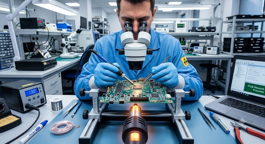
PCB rework is performed when an electronic assembly does not conform to its approved design, workmanship criteria, or production requirements but can potentially be restored without creating an unacceptable reliability risk.
Typical rework activities include:
- Removing an incorrect or damaged component
- Preparing the component site
- Installing an approved replacement
- Correcting solder-joint conditions
- Restoring coating or mechanical features
- Inspecting the reworked area
- Repeating affected electrical and functional tests
- Recording the complete rework history
The current IPC-7711/21D guidance provides procedures for the rework, repair, and modification of printed board assemblies. The standard addresses process selection, tools, materials, handling, component removal, land preparation, installation, and repair operations.
PCB rework vs. repair vs. touch-up
Although these terms are sometimes used interchangeably, they do not have exactly the same meaning.
| Term | Purpose | Example |
|---|---|---|
| Rework | Restore the assembly to its original approved requirements | Replace an incorrect component with the specified MPN |
| Repair | Restore functionality through an approved method that may differ from the original design | Install an approved jumper to restore a damaged conductor |
| Touch-up | Correct a localized workmanship condition | Add or reshape solder at a joint |
| Modification | Change the approved configuration | Change a component value under an ECO |
| Scrap | Remove the assembly from usable production | Reject a board with carbonized laminate |
The distinction matters because each action may require a different approval authority, work instruction, acceptance standard, inspection plan, and customer notification.
A modification or repair that changes the released design should follow a controlled Engineering Change Order process, rather than being treated as routine production rework.
When Is PCB Rework Appropriate?
Not every defective assembly should automatically be reworked.
Conditions that may be suitable for controlled rework include:
- Missing component
- Incorrect component
- Reversed polarity
- Misaligned component
- Solder bridge
- Insufficient solder
- Open solder joint
- Lifted component lead
- Damaged connector
- Incorrectly programmed device
- Localized workmanship defect
- Approved engineering modification
Additional examples and causes are discussed in SHDC’s guides to common PCB assembly defects and soldering defects in SMT and wave soldering.
Conditions required before approving rework
Rework should begin only when:
- The nonconformance has been clearly identified.
- An authorized disposition has been issued.
- A suitable rework procedure exists.
- The location is accessible without uncontrolled damage.
- The board condition remains acceptable.
- The replacement part is approved.
- Qualified personnel and suitable equipment are available.
- Post-rework inspection and testing can be completed.
- The resulting reliability risk is acceptable.
The decision should consider technical feasibility, product risk, customer requirements, rework history, and the value of the assembly.
When failure analysis should come first
The original board should be preserved for investigation before rework when:
- The defect is intermittent.
- The same problem has occurred repeatedly.
- The component failure mechanism is unknown.
- The board was returned from the field.
- There are signs of electrical or thermal overstress.
- Rework could destroy evidence.
- The affected lot has not been identified.
- A customer complaint or CAPA may be required.
Simply replacing the suspected component may restore one assembly while leaving the systemic cause unresolved.
PCB Rework Authorization and Disposition
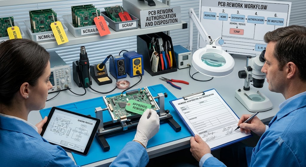
The PCB rework process should start with a documented disposition, not an operator’s informal decision.
Information required before work begins
The rework record should identify:
- Product name and part number
- PCB or PCBA revision
- Serial number or production lot
- Defect location and reference designator
- Description of the nonconformance
- Inspection or test result
- Failure-analysis reference when applicable
- Approved disposition
- Customer approval when required
- Applicable work instruction
- Required acceptance criteria
- Post-rework inspection and test requirements
A clear record prevents the wrong board, component, or revision from being processed.
Who should authorize rework?
Depending on the quality agreement and product risk, authorization may come from:
- Manufacturing engineering
- Quality engineering
- Product engineering
- Material Review Board
- Program management
- Customer or OEM representative
Operators should not select substitutions, change conductor routing, or redefine acceptance criteria without the required engineering authority.
Product-specific work instructions
A controlled work instruction should define:
- Component or location to be reworked
- Approved replacement part
- Required tools and materials
- ESD controls
- Board support
- Heating method
- Protection of adjacent components
- Process sequence
- Inspection method
- Retest requirements
- Stop and rejection criteria
- Required documentation
The procedure must be appropriate for the board construction, component package, solder alloy, thermal mass, and available equipment.
Operator qualification
Rework personnel should understand:
- ESD handling
- Component identification
- Polarity and orientation
- Thermal risks
- Equipment operation
- Site preparation
- Workmanship criteria
- Inspection requirements
- Conditions that require work to stop
IPC’s rework and repair program covers product classifications, skill levels, tools, component removal, land preparation, component installation, and printed-board repair. It is intended for technicians who already have relevant knowledge and practical experience.
Preparing the PCB for Rework
Good preparation reduces the risk of correcting one defect while creating another.
Verify the product and replacement component
Before applying heat, confirm:
- Product and board revision
- Reference designator
- Original component
- Approved replacement MPN
- Package and footprint
- Value or rating
- Polarity
- Pin 1 orientation
- Approved Vendor List status
- Product variant
The BOM, assembly drawing, schematic, and nonconformance record should agree.
Document the original condition
The manufacturer should record:
- Images of the area before rework
- Existing solder condition
- Visible damage
- Pad and solder-mask condition
- Coating or adhesive
- Original test failure
- Previous rework evidence
- Relevant serial and lot information
This information helps distinguish original defects from damage introduced during rework.
ESD workstation controls
Sensitive components should be processed in an appropriate ESD-controlled area using grounded personnel, verified work surfaces, suitable packaging, and ESD-safe tools.
ANSI/ESD S20.20 provides a framework for establishing and maintaining an ESD control program for susceptible electronic parts, assemblies, and equipment.
Board support and component protection
The rework setup should consider:
- Board thickness and size
- Bottom-side components
- Heavy copper areas
- Tall components
- Plastic connectors
- Heat-sensitive parts
- Adhesives
- Conformal coating
- Nearby solder joints
- Mechanical fixtures
- Thermal shields
Inadequate support may allow the board to bend during heating or component removal.
Moisture and thermal history
The team should review:
- Component moisture-sensitivity level
- Storage history
- Floor-life status
- Moisture-barrier packaging
- Previous reflow exposure
- Previous rework events
- Applicable baking requirements
IPC/JEDEC J-STD-033 applies to handling moisture- and reflow-sensitive devices and specifically includes components exposed to localized hot-air rework. Moisture combined with rapid heating can contribute to cracking or delamination within susceptible packages.
A single baking time or temperature should not be assumed for every component. Requirements must follow the approved component and process documentation.
Selecting the PCB Rework Method
The correct method depends on the assembly rather than operator preference.
Important factors include:
- Component package
- Lead pitch and count
- Thermal mass
- Pad configuration
- Board thickness
- Copper distribution
- Bottom-side components
- Nearby heat-sensitive parts
- Solder alloy
- Coating or adhesive
- Available equipment
- Inspection coverage
Localized vs. broader heating
Localized heating limits the area directly exposed to heat, but it may create large thermal gradients in boards with heavy copper or significant thermal mass.
Preheating or bottom-side heating may help create a more controlled thermal condition. However, the process must also protect components on both sides of the board.
Manual vs. controlled equipment
| Rework method | Typical application | Primary concern |
|---|---|---|
| Hand soldering tools | Simple accessible joints and components | Operator variation |
| Hot-air equipment | SMD removal and replacement | Heating of adjacent components |
| Controlled rework station | BGA, QFN, or complex packages | Profile development and setup |
| Vacuum desoldering equipment | Through-hole components | Pad and plated-barrel damage |
| Mechanical extraction fixture | Press-fit or secured parts | Hole and board damage |
No method is universally suitable for every component or product class.
Component Removal During PCB Rework
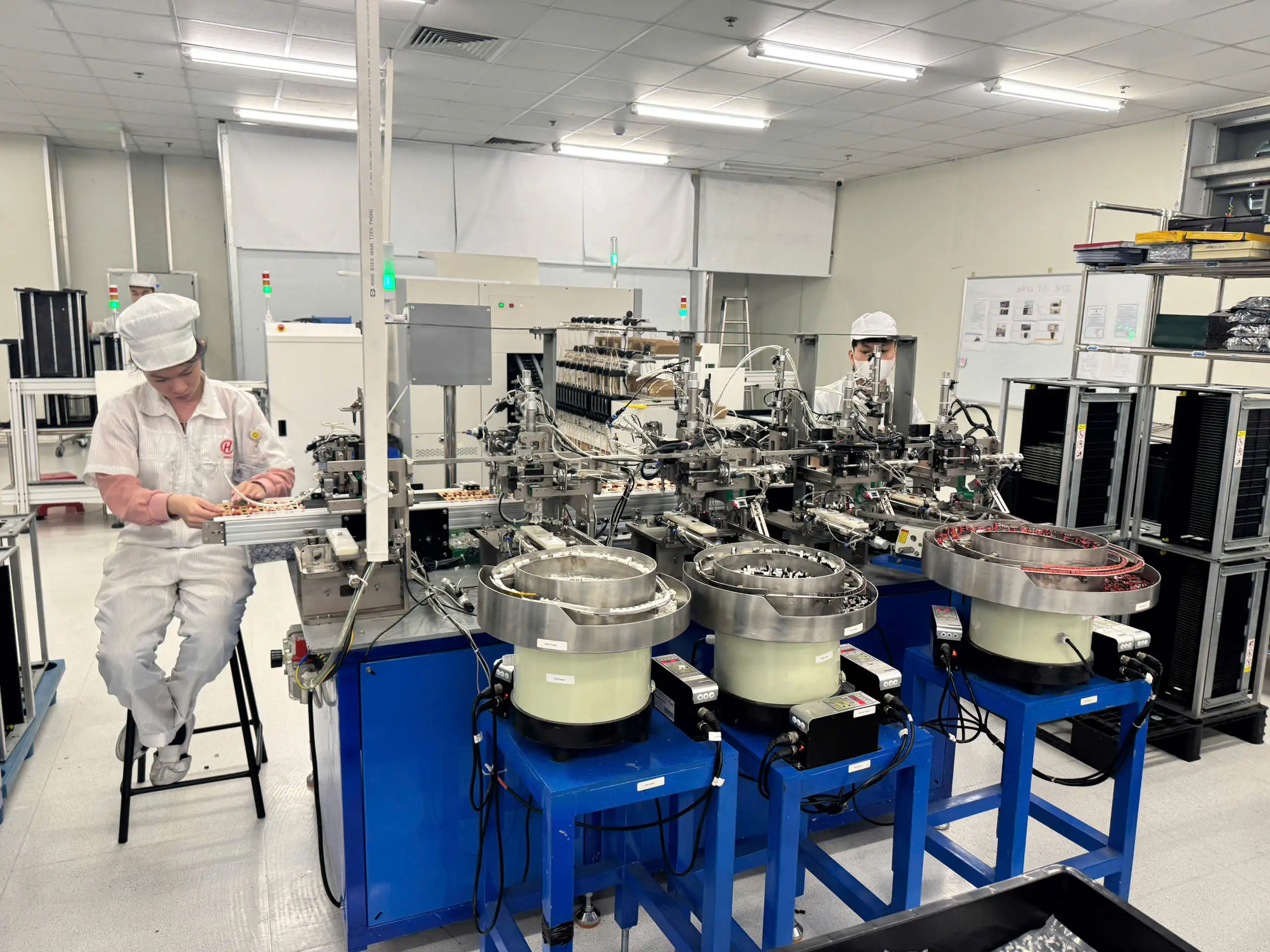
Removing the component is often the highest-risk stage because the solder must be fully released before mechanical force is applied.
Small passive components
Chip resistors, capacitors, and similar parts require controlled heating and careful handling to prevent:
- Pad lifting
- Solder-mask damage
- Movement of adjacent components
- Cracking of ceramic parts
- Excess solder on the site
- Incorrect removal of a nearby RefDes
Leaded surface-mount packages
For SOIC, TSSOP, QFP, and other leaded packages, the process should ensure all leads reach the required solder condition before the package is lifted.
Potential risks include:
- Bent leads
- Torn pads
- Solder bridges
- Damage to fine-pitch lands
- Uneven heating
- Excessive thermal exposure
QFN and other bottom-terminated components
QFN, DFN, and LGA packages present additional challenges because their joints and thermal pads are underneath the component.
The manufacturer must consider:
- Hidden solder connections
- Thermal-pad area
- Site flatness
- Solder removal
- Package alignment
- Inspection limitations
- X-ray availability
BGA removal
A BGA removal procedure should control:
- Board support
- Top and bottom heating
- Package temperature
- Solder release
- Package lifting
- Pad protection
- Nearby-component exposure
- Moisture condition
- Underfill or adhesive where present
The package should not be mechanically forced from the board before all joints are released.
Through-hole component removal
Removing a multi-pin connector or through-hole component may require solder evacuation from several plated-through holes.
Risks include:
- Barrel damage
- Lifted lands
- Blocked holes
- Connector deformation
- Excessive board heating
- Damage to internal connections
- Mechanical stress during extraction
Press-fit or mechanically secured parts
Press-fit components and mechanically fastened assemblies may require dedicated fixtures. Uncontrolled pulling can deform holes, damage plating, or bend the PCB.
Pad Cleaning and Site Preparation
After component removal, the site must be evaluated before a replacement part is installed.
Remove residual solder
The objective is to create a clean, controlled, and sufficiently flat surface without damaging the lands.
The process should avoid:
- Excess pressure
- Repeated unnecessary heating
- Pulling on partially attached pads
- Scratching conductors
- Removing solder mask
- Contaminating nearby areas
Clean flux and contamination
The cleaning method must be compatible with:
- The soldering materials
- PCB laminate
- Components
- Labels
- Adhesives
- Conformal coating
- Customer cleanliness requirements
The site should be dry and free from loose material before inspection.
Inspect pads and conductors
Inspect for:
- Lifted or missing pads
- Torn conductors
- Solder-mask damage
- Exposed laminate
- Cracks near vias
- Delamination
- Blistering
- Carbonization
- Discoloration
- Irregular site flatness
A damaged pad should not automatically be repaired under the same rework disposition. Conductor or land repair may require a separate approved procedure and customer authorization.
Decide whether the site remains reworkable
Stop the process when:
- Pad adhesion is uncertain.
- A conductor has been damaged beyond the approved limit.
- Laminate damage is visible.
- Carbonization is present.
- The required joint cannot be inspected.
- The board cannot be adequately retested.
- The proposed action exceeds the approved disposition.
Proceeding despite these conditions may convert a manageable defect into an uncontrolled reliability risk.
Installing the Replacement Component
Verify the replacement part
Before installation, verify:
- Manufacturer
- Manufacturer part number
- Package
- Value or electrical rating
- Product grade
- Lot or date code
- Approved substitution status
- Polarity
- Pin configuration
- Moisture condition
A visually similar component is not necessarily an acceptable replacement.
Apply approved soldering materials
The solder, paste, flux, or other material should be:
- Approved for the product
- Compatible with the original process
- Within its controlled use condition
- Applied in a suitable quantity
- Traceable when required
Excess material may cause bridging or contamination, while insufficient material may produce weak or open joints.
Align and place the component
Confirm:
- Correct RefDes
- Pin 1
- Polarity
- Lead-to-pad alignment
- Package centering
- Mechanical seating
- Connector orientation
- Clearance from adjacent components
Control heating and cooling
The developed process should account for:
- Board thermal mass
- Component body
- Solder alloy
- Adjacent-component limits
- Heating rate
- Peak condition
- Time at temperature
- Cooling
- Board support
The component should remain stable while the solder solidifies. Manual movement during cooling may create disturbed joints.
BGA and QFN Rework Controls
BGA and QFN rework requires additional controls because most solder joints cannot be fully inspected visually.
Why hidden-joint rework is more difficult
Challenges include:
- Joints located beneath the package
- Uneven board and package heating
- Warpage
- Hidden pad damage
- Thermal-pad solder control
- Nearby-component exposure
- Limited visual evidence
- Need for specialized inspection
Reballing vs. replacement
A removed BGA may be reballed or replaced, depending on:
- Approved procedure
- Component condition
- Customer requirements
- Product risk
- Package handling history
- Economic feasibility
Reuse should not be assumed to be acceptable for every product.
Thermal-profile development
The process should be developed around:
- Board thickness
- Copper distribution
- Package dimensions
- Solder alloy
- Bottom heating
- Equipment capability
- Moisture status
- Temperature-sensitive neighboring components
IPC-7711/21D includes process considerations for rework and repair, while J-STD-033 addresses moisture-sensitive devices exposed to localized heating.
Post-rework X-ray inspection
X-ray may be used to evaluate:
- Package alignment
- Solder bridges
- Missing or insufficient solder
- Ball distribution
- Voiding
- Selected open-joint indications
X-ray does not replace electrical or functional testing. Some cracks or interface conditions may also require other analytical methods.
Reasons to reject hidden-joint rework
The assembly should not be released when there is:
- Unresolved misalignment
- Evidence of pad damage
- Excessive board warpage
- Unacceptable solder condition
- Unresolved X-ray findings
- Failed electrical testing
- Thermal exposure outside the approved process
Through-Hole and Connector Rework
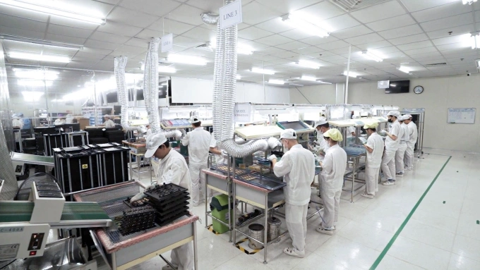
Clear the plated-through holes
Residual solder must be removed without damaging the barrel or annular ring.
Do not force replacement leads into obstructed holes. Mechanical force can damage plating or internal connections.
Inspect the through-hole site
Check:
- Barrel condition
- Land adhesion
- Annular ring
- Hole obstruction
- Laminate condition
- Cracks
- Signs of overheating
Install and align the replacement
Confirm:
- Part identity
- Orientation and polarity
- Seating
- Lead insertion
- Connector height
- Mechanical alignment
- Board-to-enclosure relationship
- Required support or fasteners
Evaluate the finished joints
Acceptance may include:
- Solder fill
- Wetting
- Lead condition
- Bridges
- Excess or insufficient solder
- Connector straightness
- Mechanical stability
The exact requirements must follow the applicable product documentation and agreed acceptance criteria.
Thermal and Mechanical Risks During PCB Rework
Rework exposes an already assembled product to additional thermal and mechanical stress.
Pad and conductor damage
Excess heat, force, or repeated handling can cause:
- Lifted pads
- Torn conductors
- Weakened pad adhesion
- Damaged vias
- Broken internal connections
Laminate and solder-mask damage
Possible signs include:
- Delamination
- Blistering
- Cracking
- Discoloration
- Solder-mask lifting
- Carbonization
Carbonized laminate generally presents a serious electrical and reliability concern and may justify scrapping the board.
Component overheating
Heat may affect:
- Plastic connectors
- Electrolytic capacitors
- LEDs
- Sensors
- Batteries
- Adhesives
- Thermal materials
- Bottom-side components
- Previously reworked components
Board warpage
Warpage can interfere with package alignment, solder formation, connector position, and mechanical fit.
Repeated thermal exposure
There is no universal number of rework cycles appropriate for every PCBA. IPC’s published guidance does not itself impose one maximum count for all assemblies; product-specific controls are still necessary.
The allowable history should consider:
- Board construction
- Component specifications
- Product class
- Previous process exposure
- Site condition
- Inspection capability
- Customer requirements
- Reliability risk
Post-Rework Inspection
A completed component replacement must pass defined inspection before electrical testing or release.
Visual and microscopic inspection
Check:
- Correct component
- Orientation and polarity
- Alignment
- Solder wetting
- Bridges
- Open or disturbed joints
- Lifted leads
- Excess solder
- Insufficient solder
- Pad and mask condition
- Cleanliness
- Adjacent-component condition
- Physical damage
The product drawing and work instruction should define which characteristics are critical.
Automated Optical Inspection
For visible joints and component features, the assembly may return to Automated Optical Inspection.
The AOI program should:
- Match the product revision.
- Include the reworked location.
- Use approved limits.
- Record the inspection result.
- Require controlled review of machine calls.
AOI cannot adequately evaluate every hidden connection or electrical characteristic.
X-ray inspection
X-ray may be appropriate after reworking:
- BGA packages
- QFN and DFN packages
- LGA packages
- Other bottom-terminated components
- Selected through-hole connections
The required coverage should be established by the product risk and quality agreement.
Coating and cleanliness restoration
Where conformal coating is present:
- Confirm the correct removal boundary.
- Clean the reworked area.
- Restore the approved coating.
- Maintain keep-out zones.
- Protect connectors and test points.
- Inspect the restored layer.
A board should not be released with an uncontrolled gap in a required protective coating.
Post-Rework Testing
Post-rework testing should cover both the replaced component and any circuit or function that may have been affected by the operation.
Continuity and electrical checks
Testing may include:
- Continuity
- Resistance
- Opens and shorts
- Power-rail checks
- Component-value verification
- Signal measurements
- Leakage
- Current consumption
In-circuit and flying-probe testing
Where test access is available, ICT or flying probe can help verify component presence, connectivity, values, opens, and shorts.
The selection depends on production volume, test access, fixture availability, and product design. SHDC’s comparison of ICT and functional testing explains the different roles of these methods.
Functional testing
Functional testing may verify:
- Power-up sequence
- Inputs and outputs
- Communication interfaces
- Firmware behavior
- Load performance
- Sensors
- Displays or indicators
- Customer-defined functions
The test program, fixture, and pass/fail limits must match the product revision.
Firmware verification
When a programmable device is replaced or reprogrammed, verify:
- Firmware version
- Checksum
- Device configuration
- Serial number
- Calibration data
- Programming result
- Security or fuse settings where applicable
Safety and stress tests
Depending on the product, required testing may include:
- High-voltage testing
- Insulation checks
- Leakage testing
- Load testing
- Aging or burn-in
- Thermal testing
- Environmental testing
These tests should only be included where required by the product specification or quality plan.
Retest the affected process path
A board should not be approved only because the replacement component passes a localized measurement.
The manufacturer should determine:
- Which previous test stages must be repeated
- Which functions could have been affected by heating
- Whether adjacent components require verification
- Whether safety tests must be repeated
- Whether the full production test sequence is required
A broader overview of inspection and electrical verification is available in SHDC’s PCBA testing guide.
PCB Rework Acceptance Criteria
Acceptance criteria should be agreed before production and applied consistently after rework.
Product-specific requirements come first
The applicable hierarchy may include:
- Contract and customer requirements
- Approved drawings and specifications
- Quality agreement
- Product-specific rework instruction
- Referenced industry standards
IPC released Revision J of both IPC-A-610 and J-STD-001 in 2024. IPC-A-610 addresses post-assembly acceptability, while J-STD-001 covers soldering processes, materials, and related requirements.
SHDC provides additional explanations of IPC-A-610 acceptance criteria and the differences between IPC J-STD-001 and IPC-A-610.
Workmanship acceptance
The inspected assembly may need to demonstrate:
- Correct part and orientation
- Acceptable solder condition
- Intact pads and conductors
- Acceptable cleanliness
- Mechanical integrity
- Correct coating restoration
- No secondary damage
Electrical and functional acceptance
The board should only be released after:
- All required inspections pass.
- Required tests pass.
- Results are recorded.
- No unresolved indications remain.
- The authorized disposition is closed.
Customer approval and deviation
OEM approval may be required when:
- The repair differs from the original design.
- A part outside the AVL is proposed.
- A conductor or land is repaired.
- The original acceptance requirement cannot be met.
- The quality agreement requires notification.
- Reliability risk has changed.
PCB Rework Traceability and Records
A complete rework record should allow the OEM and manufacturer to reconstruct what happened to the board.
Information to record
The record may include:
- Product part number
- Revision
- Serial number or production lot
- Defect type
- Reference designator
- Removed component
- Replacement component
- Replacement lot or date code
- Operator
- Date and workstation
- Equipment
- Work-instruction revision
- Inspection result
- Test result
- Approval
- Previous rework history
Link rework to production data
Where applicable, the record should connect to:
- Original production lot
- Initial inspection results
- Test failure
- Nonconformance report
- Failure-analysis record
- CAPA
- Material lot
- Shipment history
A structured traceability system in electronics manufacturing helps determine whether repeated defects are associated with a specific component lot, operator, process, or product revision.
Why traceability matters to US OEMs
Traceability supports:
- Field-return investigation
- Identification of repeat defects
- Containment of affected lots
- Review of rework frequency
- Operator and process trend analysis
- Customer reporting
- Reliability monitoring
A reworked board should not become indistinguishable from an assembly with no rework history when the quality agreement requires that information.
When Should a PCB Be Scrapped Instead of Reworked?
Rework should not continue indefinitely simply because the board has high material value.
| Board condition | Possible disposition |
|---|---|
| Localized, accessible solder defect | Controlled rework may be suitable |
| Damaged pad with an approved repair method | Engineering or MRB review |
| Multiple previous reworks | Reliability review or scrap |
| Carbonized laminate | Scrap |
| Serious delamination | Scrap |
| Unknown thermal history | Risk review or scrap |
| Required inspection cannot be performed | Do not release |
| Required testing cannot be completed | Do not release |
| Customer prohibits the proposed repair | Scrap or return for disposition |
Other scrap indicators include:
- Severe conductor damage
- Unrecoverable plated-through-hole damage
- Excessive board warpage
- Multiple damaged areas
- Unacceptable contamination
- Untraceable replacement materials
- Rework cost exceeding board value
- Reliability risk that cannot be demonstrated as acceptable
The decision should be documented by the authorized engineering or quality function.
Common PCB Rework Mistakes
| Mistake | Risk | Recommended control |
|---|---|---|
| Reworking before failure analysis | Original evidence is lost | Preserve and investigate first |
| Installing the wrong replacement | New functional or reliability issue | Verify BOM, MPN, and AVL |
| Using uncontrolled heat | Pad, laminate, or component damage | Use an approved process |
| Failing to support the PCB | Warpage and mechanical stress | Use suitable support or fixture |
| Ignoring nearby components | Secondary thermal damage | Define protection requirements |
| Inadequate site preparation | Weak or misaligned joints | Inspect and prepare the site |
| Skipping hidden-joint inspection | Undetected BGA or QFN defects | Use risk-based X-ray |
| Testing only the new component | Related circuits may remain faulty | Retest the affected process path |
| Failing to restore coating | Environmental protection is reduced | Restore and inspect the coating |
| No rework record | Traceability is lost | Link the record to serial or lot |
| Unlimited repeat rework | Accumulated thermal damage | Define review and scrap criteria |
PCB Rework Audit Checklist for US OEMs

When evaluating a PCBA supplier, ask:
| Audit question | Evidence to request |
|---|---|
| Who authorizes rework? | Disposition and approval records |
| Are operators qualified? | Training and competency records |
| Are procedures product-specific? | Controlled work instructions |
| How is the replacement verified? | BOM, AVL, barcode, or material record |
| How is thermal exposure controlled? | Approved profile and equipment data |
| How are adjacent components protected? | Setup plan or work instruction |
| How are pads inspected? | Inspection criteria and images |
| Is hidden-joint rework X-rayed? | X-ray reports where applicable |
| Which tests are repeated? | Post-rework test plan and records |
| Is history linked to the serial number? | MES, traveler, or traceability record |
| Is repeat rework limited? | MRB and scrap criteria |
| When is OEM approval required? | Quality agreement or deviation process |
| How is coating restored? | Coating procedure and inspection record |
| How do repeat defects trigger CAPA? | NCR, trend, and CAPA records |
Rework capability should be evaluated together with supplier quality, testing, change management, and documentation controls—not as a standalone technician skill.
PCB Rework Within the Manufacturing Quality System
Rework should correct isolated nonconforming assemblies, not compensate for an unstable manufacturing process.
A mature quality system monitors:
- Rework rate
- Rework location
- Defect type
- Operator or production line
- Component lot
- Product revision
- Test results after rework
- Repeat failures
- Customer returns involving reworked boards
A rising rework rate should trigger investigation of the original process. Corrective actions may require updates to:
- Control plans
- Work instructions
- Machine programs
- Inspection limits
- Reflow profiles
- Fixtures
- BOM or AVL
- Design documentation
These controls are part of a broader quality assurance and inspection system in EMS.
PCB Rework and Testing at SHDC
SHDC’s company profile states that the company provides EMS activities from component soldering, assembly, and testing through final packaging. Its documented production flow includes AOI, repair, ICT, visual inspection, FCT, OQC, and packaging.
The profile also lists production and test equipment including 3D AOI, Kyoritsu ICT, wave soldering, nitrogen reflow, high-voltage testing, aging testing, and functional-testing equipment.
These documented checkpoints can support inspection and verification after approved production rework. However, rework requirements remain product-specific. BGA rework, X-ray inspection, coating restoration, special repairs, and customer-specific acceptance conditions should be confirmed during technical review rather than assumed from general factory capability.
US companies evaluating manufacturing options can review SHDC’s broader PCBA Vietnam capabilities and its guide to qualifying a PCB assembly Vietnam supplier.
Conclusion
A reliable PCB rework process begins with authorization and ends only after inspection, testing, documentation, and formal release.
Component removal is just one stage. The manufacturer must also verify the replacement part, protect the assembly from ESD and thermal damage, prepare and inspect the component site, control installation, restore protective materials, and repeat every affected test.
For US OEMs, the most important supplier questions are not simply whether a factory can replace a component. The supplier should demonstrate who approves rework, how operators are qualified, how thermal exposure is controlled, which acceptance criteria apply, what tests are repeated, how rework is traced, and when a board must be scrapped.
Frequently Asked Questions
What is the PCB rework process?
The PCB rework process is a controlled sequence used to restore a nonconforming assembly to its approved requirements. It normally includes authorization, component removal, site preparation, replacement, inspection, testing, documentation, and release.
What is the difference between PCB rework and repair?
Rework restores the assembly to its original requirements. Repair may restore functionality through an approved method that differs from the original design, such as a conductor jumper.
Can every PCB be reworked?
No. Reworkability depends on the defect, board construction, pad condition, component package, thermal history, available equipment, test coverage, and customer requirements.
Which components are difficult to rework?
BGA, QFN, DFN, LGA, fine-pitch ICs, high-thermal-mass connectors, and multi-pin through-hole components generally require more process control and specialized equipment.
Is X-ray required after BGA rework?
X-ray is commonly used to evaluate hidden BGA solder connections, but the exact requirement depends on the product specification, risk assessment, and approved quality plan.
How is a PCB tested after rework?
Testing may include visual inspection, AOI, X-ray, continuity, resistance checks, ICT, flying probe, functional testing, firmware verification, safety testing, or stress testing, depending on the affected area.
How many times can a PCB be reworked?
There is no universal number suitable for every PCB. Limits should be based on the board condition, thermal history, component requirements, product class, inspection capability, and customer approval.
When should a reworked PCB be scrapped?
A board should be considered for scrap when it has serious pad or conductor damage, delamination, carbonization, excessive warpage, uncontrolled thermal history, repeated rework, or cannot pass the required inspection and testing.
What standards apply to PCB rework?
Commonly referenced documents include IPC-7711/21D for rework, modification, and repair procedures; IPC-A-610J for assembly acceptability; and IPC J-STD-001J for soldering process and material requirements. The applicable revision and product class should be agreed before production.
Should reworked PCBAs be traceable?
Yes. The record should identify the product, serial number or lot, defect, component location, removed and replacement parts, operator, procedure, inspection, testing, and approval.